3D NAND memory and method for forming same

A 3DNAND, memory technology, applied in the direction of electric solid-state devices, semiconductor devices, electrical components, etc., can solve problems such as storage structure failure, and achieve the effect of preventing failure

Active Publication Date: 2019-05-31
YANGTZE MEMORY TECH CO LTD
View PDF5 Cites 10 Cited by
  • Summary
  • Abstract
  • Description
  • Claims
  • Application Information

AI Technical Summary

Problems solved by technology

[0004] In order to further increase the storage capacity, when forming the stack structure in the prior art, a multi-layer stack structure is usually formed, and each layer stack structure includes several alternately stacked sacrificial layers and isolation layers. In the multi-layer stack structure A channel hole is formed; a storage structure is formed in the channel hole, but this storage structure still has the problem of failure

Method used


Image

  • 3D NAND memory and method for forming same
  • 3D NAND memory and method for forming same
  • 3D NAND memory and method for forming same

Examples


Embodiment Construction

[0038] As mentioned in the background, the existing multi-layer stacked 3D NAND memory has the problem of failure.

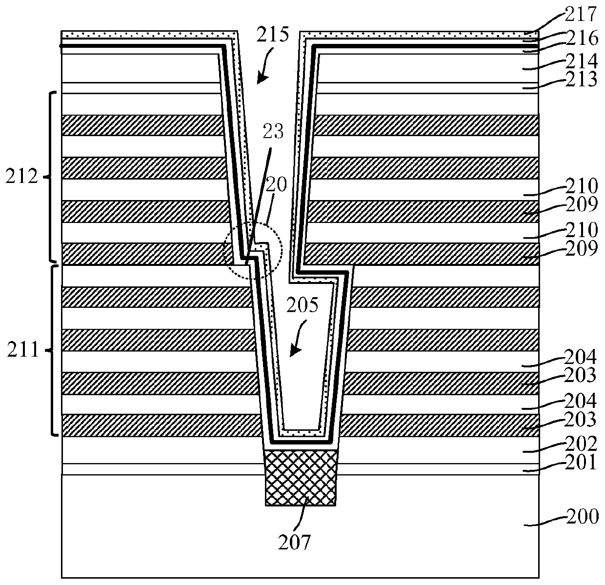
[0039] The study found that the location where the failure problem of multi-layer stacked 3D NAND memory generally occurs at the junction of the multi-layer stacked structure, please refer to figure 2 20 positions indicated by the dotted box in .

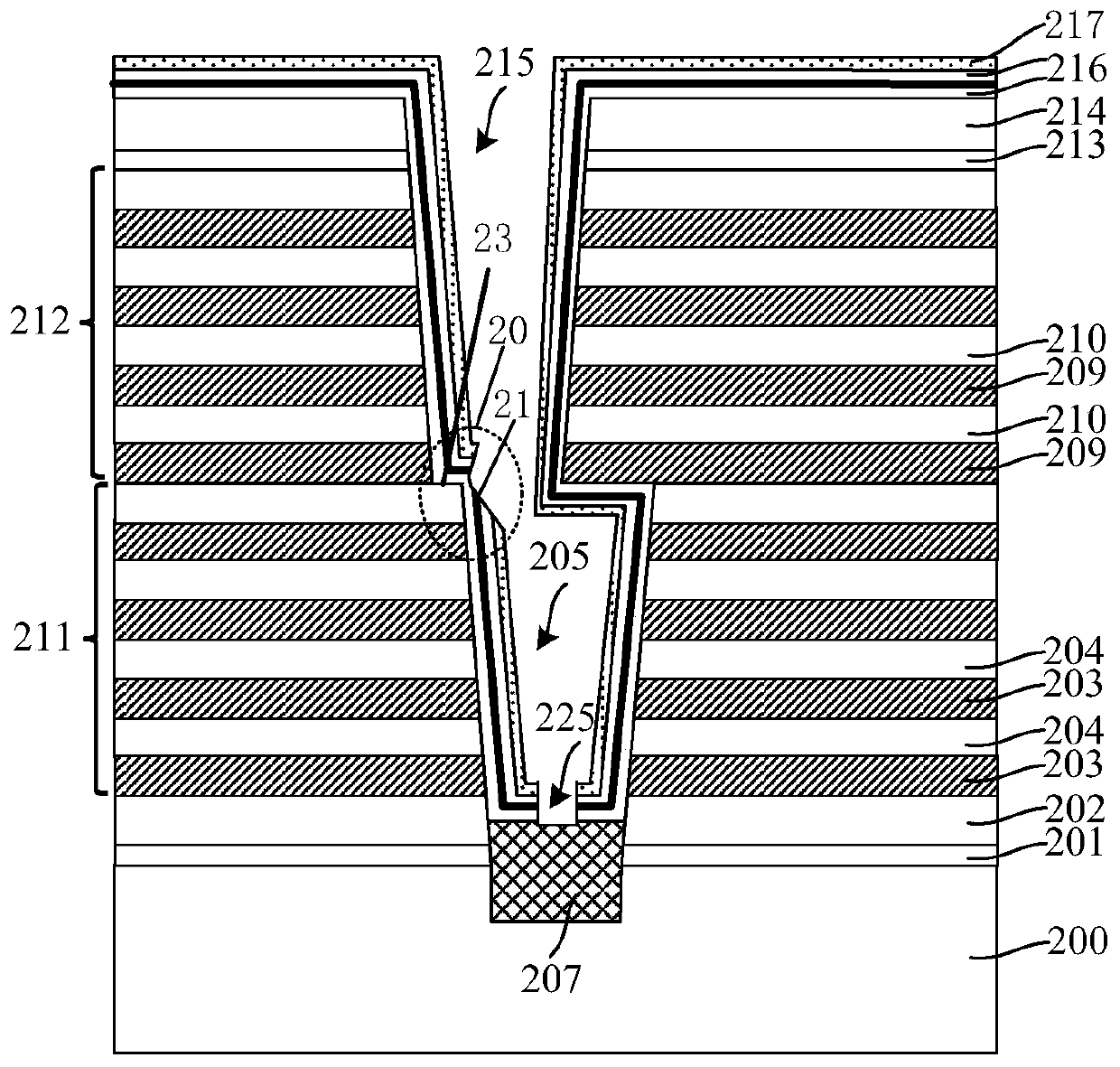
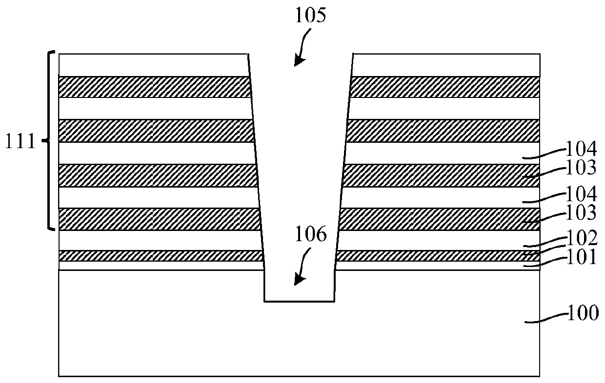
[0040] After further research, the specific reasons for the above problems are: Figure 1-2 It is a schematic diagram of the cross-sectional structure of the formation process of the 3D NAND memory according to an embodiment of the present invention. First, please refer to figure 1, forming a first stack structure 211 on the semiconductor substrate 200, the first stack structure 211 includes a number of alternately stacked sacrificial layers 203 and insulating layers 204, the first stack structure 211 and the semiconductor substrate 200 can also be Form a buffer oxide layer 201 and a dielectric layer 202; etch the...


PUM


Abstract

A 3D NAND memory and a method for forming the same are disclosed. The forming method includes providing a semiconductor substrate on which a stacked structure is formed, wherein the stacked structureincludes a plurality of sacrificial layers and isolation layers which are alternately stacked, the stacked structure has a first channel hole and a second channel hole in communication with the firstchannel hole, the second channel hole has an alignment offset with respect to the first channel hole, and a step is formed at a boundary between the first channel hole and the second channel hole; forming a charge storage layer on the sidewalls and the bottoms of the first channel hole and the second channel hole; forming a channel hole sacrificial layer on the charge storage layer; forming a protective layer on the channel hole sacrificial layer; successively etching the protective layer, the channel hole sacrificial layer, and the charge storage layer on the bottom of the first channel holeto form an opening exposing the surface of the semiconductor epitaxial layer. The method of the present invention prevents the charge storage layer at the step from being broken or damaged, thereby preventing memory failure.

Description

technical field [0001] The invention relates to the field of semiconductor manufacturing, in particular to a 3D NAND memory and a forming method thereof. Background technique [0002] NAND flash memory is a better storage device than hard disk drives, and it has been widely used in electronic products as people pursue non-volatile storage products with low power consumption, light weight and high performance. At present, the NAND flash memory with a planar structure is close to the limit of practical expansion. In order to further increase the storage capacity and reduce the storage cost per bit, a 3D NAND memory with a 3D structure is proposed. [0003] The manufacturing process of the existing 3D NAND memory includes: providing a substrate on which a stacked structure in which isolation layers and sacrificial layers are alternately stacked; etching the stacked structure to form an exposed substrate surface in the stacked structure channel hole; form a storage structure in...

Claims


Application Information

Patent Timeline
Patent Type & Authority Applications(China)
IPC IPC(8): H01L27/11585
Inventor 霍宗亮薛家倩
Owner YANGTZE MEMORY TECH CO LTD
Why Eureka
Try Eureka