Preparation method of ultrathin wafer

A wafer, ultra-thin technology, applied in semiconductor/solid-state device manufacturing, electrical components, circuits, etc., can solve problems such as large fluctuation range, difficult control of wafer thickness range, and limited application range, so as to achieve a wide range of applications and avoid Problems of debris and cracks, the effect of simple process structure

Pending Publication Date: 2019-06-04
浙江荷清柔性电子技术有限公司
View PDF2 Cites 7 Cited by
  • Summary
  • Abstract
  • Description
  • Claims
  • Application Information

AI Technical Summary

Problems solved by technology

[0004] Based on this, it is necessary to provide a wafer with a simple process structure, controllable thickness fluctuation range, and a wide range of applications in view of the problems that the wafer thic

Method used


Image

  • Preparation method of ultrathin wafer
  • Preparation method of ultrathin wafer
  • Preparation method of ultrathin wafer

Examples


Embodiment Construction

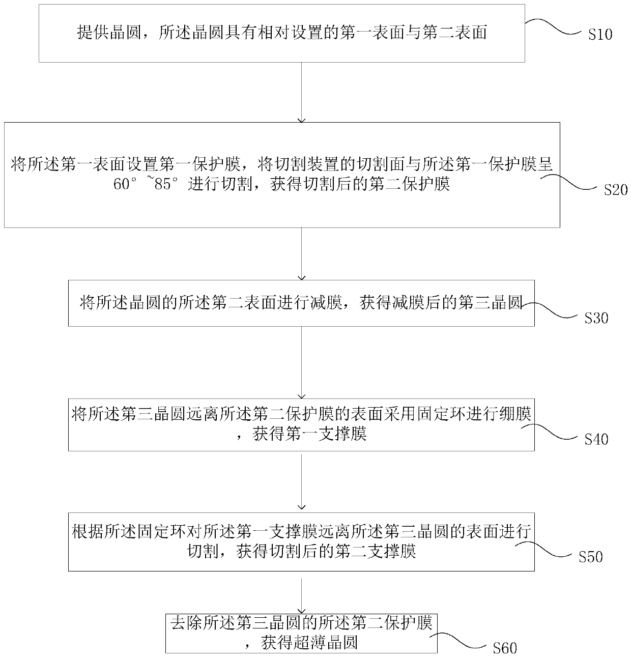
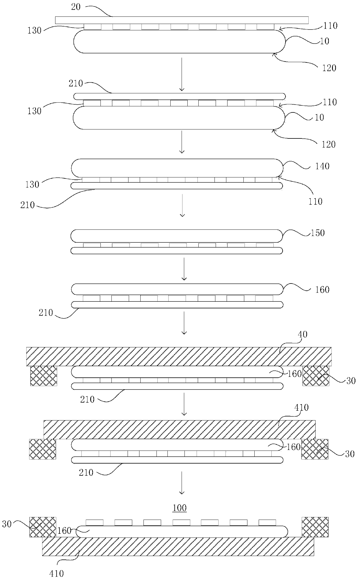
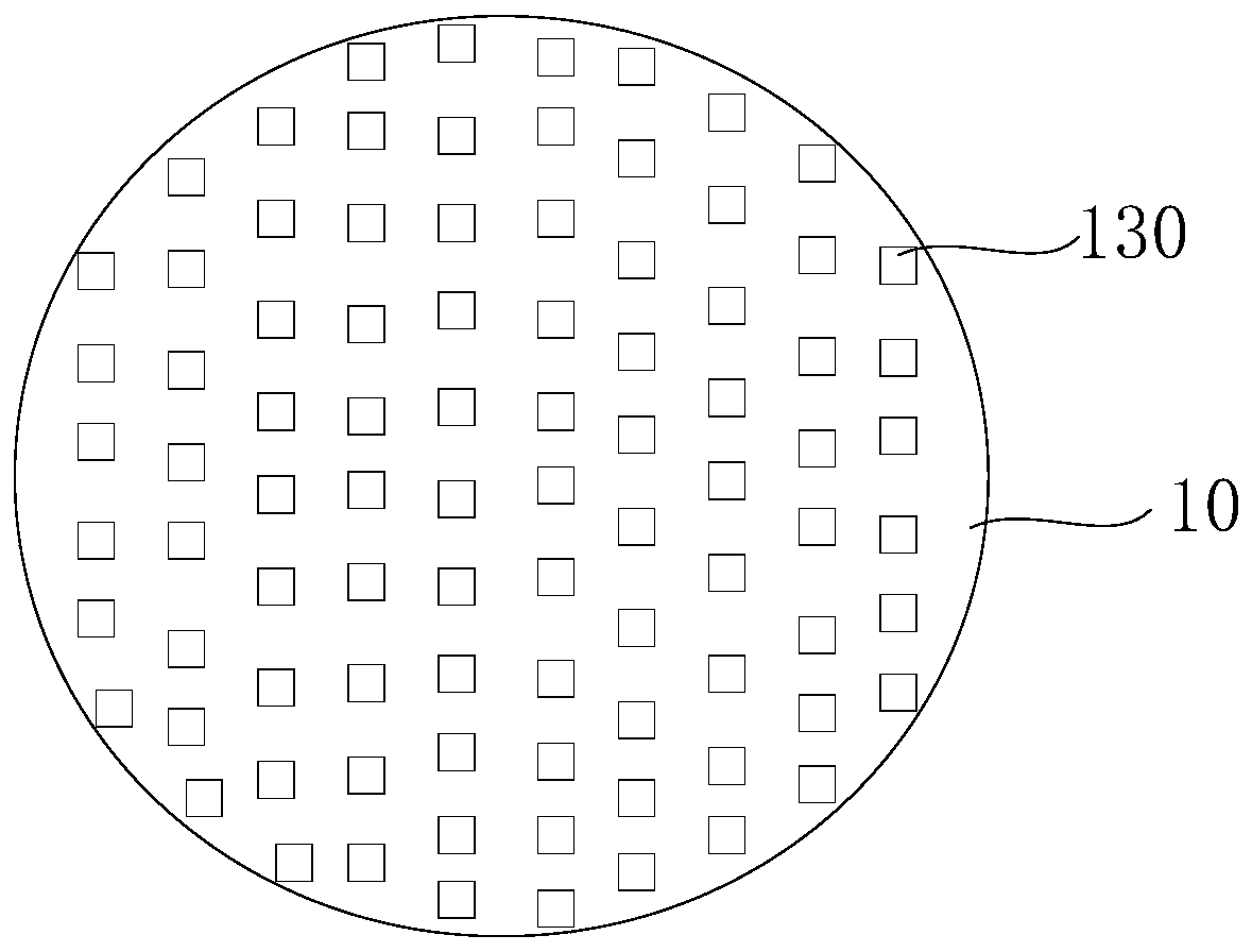
[0040] In order to make the purpose, technical solution and advantages of the present application clearer, the present application will be further described in detail through the following embodiments and in conjunction with the accompanying drawings. It should be understood that the specific embodiments described here are only used to explain the present application, not to limit the present application.

[0041] The serial numbers assigned to components in this document, such as "first", "second", etc., are only used to distinguish the described objects, and do not have any sequence or technical meaning. The "connection" and "connection" mentioned in this application all include direct and indirect connection (connection) unless otherwise specified. In the description of this application, it should be understood that the terms "upper", "lower", "front", "rear", "left", "right", "vertical", "horizontal", "top", The orientation or positional relationship indicated by "bottom"...


PUM

PropertyMeasurementUnit
Diameteraaaaaaaaaa
Thicknessaaaaaaaaaa
Thicknessaaaaaaaaaa

Abstract

The invention provides a preparation method of an ultrathin wafer. According to the preparation method, the technical structure is simple, the wafer is thinned directly after that first surface film pasting, turnover time of the process is short, and coarse grinding according to the first preset thickness, fine grinding according to the second preset thickness and dry-method polishing according tothe third preset thickness are carried out to control the range of thickness fluctuation. Cutting is carried out with support of a scribing iron hoop after that the wafer is thinned, a second protective film is removed, and thus, the ultrathin wafer is supported, and avoided fro, fragment and crack in the transfer process due to being too thin. The scribing iron hoop is used to stretch the film after thinning, different scribing adhesive films are selected according to requirements for chip packaging manners, and the application range is wide.

Description

technical field [0001] The present application relates to the field of semiconductor manufacturing, in particular to a method for preparing an ultra-thin wafer. Background technique [0002] At present, with the increasing demand for electronic devices in the market, the rapid development of electronic device processing technology has been driven. Especially since the advent of flexible electronics, research on the production process of flexible electronics has been increasing. Flexible electronics have broad application prospects in information, energy, medical, national defense and other fields due to their unique flexibility and ductility, as well as high-efficiency and low-cost manufacturing processes. Compared with traditional electronic devices, flexible electronics requires chips to have a certain ability to adapt to curved surfaces. When the thinning thickness is less than 50um, the ultra-thin wafer has good flexible bending ability and good mechanical stability. ...

Claims


Application Information

Patent Timeline
IPC IPC(8): H01L21/683H01L21/78
Inventor 刘东亮缪炳有滕乙超魏瑀
Owner 浙江荷清柔性电子技术有限公司
Why Eureka
Try Eureka