A chemical vapor deposition device including a Raman spectroscopy in-situ measurement chamber

A technology of chemical vapor deposition and Raman spectroscopy, which is applied in the field of chemical vapor deposition devices, achieves the effects of high sensitivity, simple analysis process and short test time

Active Publication Date: 2019-10-22
WUHAN UNIV
View PDF6 Cites 0 Cited by
  • Summary
  • Abstract
  • Description
  • Claims
  • Application Information

AI Technical Summary

Problems solved by technology

[0004] In order to solve the above problem, the present invention provides a chemical vapor deposition device including a Raman spectroscopy in-situ measurement cavity, which solves the problem of in-situ Raman detection of the film without affecting the growth of the film, and then adjusts the process in real time to reduce defects

Method used


Image

  • A chemical vapor deposition device including a Raman spectroscopy in-situ measurement chamber
  • A chemical vapor deposition device including a Raman spectroscopy in-situ measurement chamber
  • A chemical vapor deposition device including a Raman spectroscopy in-situ measurement chamber

Examples


Embodiment Construction

[0026] The following will clearly and completely describe the technical solutions in the embodiments of the present invention with reference to the accompanying drawings in the embodiments of the present invention. Obviously, the described embodiments are only a part of the present invention, not all embodiments. Based on the embodiments of the present invention, all other embodiments obtained by persons of ordinary skill in the art without making creative efforts belong to the protection scope of the present invention.

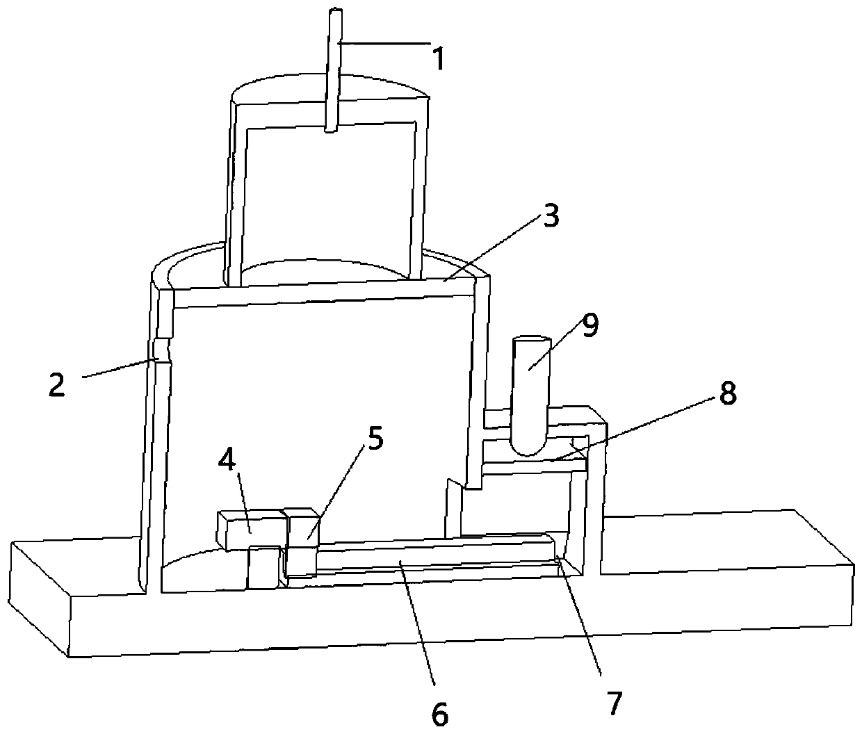
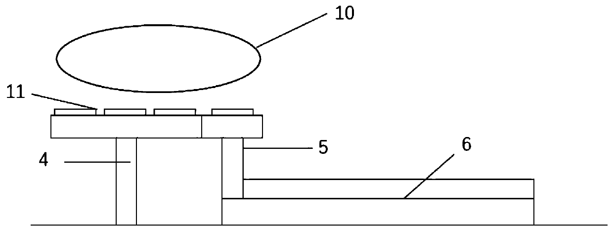
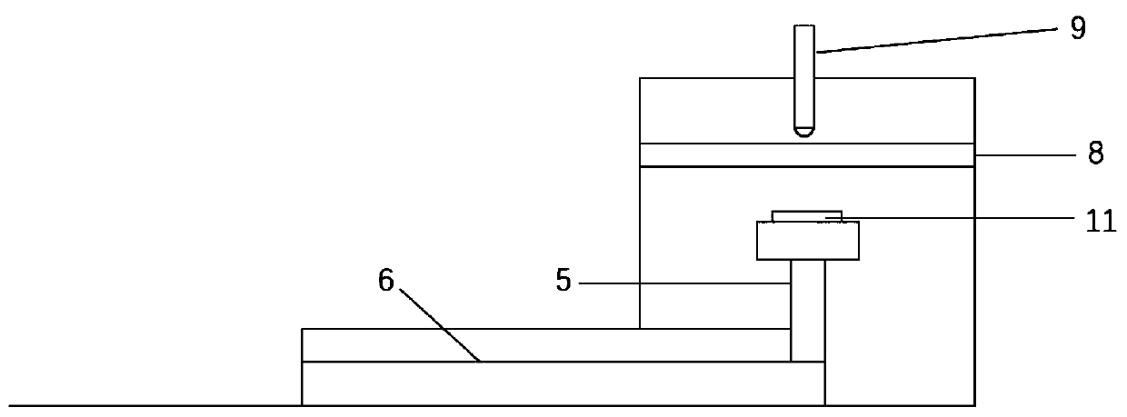
[0027] Such as Figure 1-3 As shown, the embodiment of the present invention provides a chemical vapor deposition device comprising a Raman spectrum in-situ measurement chamber, which includes a transmission device 6, a reaction chamber for performing a chemical vapor deposition reaction on a thin film material 11, and a reaction chamber for performing a chemical vapor deposition reaction on a thin film material 11. The film material 11 is a monitoring chambe...


PUM


Abstract

The present invention relates to a chemical vapor deposition device comprising a Raman spectroscopy in-situ measurement cavity. The device comprises a transmission device, a reaction cavity for performing chemical vapor deposition reaction on a thin film material and a monitoring cavity for performing Raman spectroscopy in-situ monitoring on the thin film material; the reaction cavity communicateswith the monitoring cavity, a reaction base is arranged in the reaction cavity, and a Raman spectroscopy monitoring module is arranged in the monitoring cavity; the reaction base is used as a substrate for film material growth; the transmission device is used for controlling the reaction base to move between the reaction chamber and the monitoring chamber; and the Raman spectroscopy monitoring module is used for performing Raman spectroscopy in-situ monitoring on the thin film material moved into the monitoring cavity. The present invention provides the chemical vapor deposition device comprising the Raman spectroscopy in-situ measurement cavity, which solves the problem of in-situ Raman detection of the thin film under the condition that the growth of the thin film is not affected, and further can adjust the process in real time to reduce defects.

Description

technical field [0001] The invention relates to a chemical vapor deposition device, in particular to a chemical vapor deposition device including a Raman spectrum in-situ measurement chamber. Background technique [0002] The third-generation semiconductor materials include diamond, silicon carbide, and gallium nitride, which have the advantages of high thermal conductivity, high breakdown field strength, high saturation electron drift rate, and high bonding energy, which can meet the requirements of modern electronic technology for high temperature, high power, and high voltage. New requirements for harsh conditions such as high frequency, high frequency and radiation resistance have important application prospects in the fields of semiconductor lighting, power electronic devices, lasers and detectors. [0003] At present, chemical vapor deposition is the main method for preparing thin films such as diamond, silicon carbide and gallium nitride, but there are some insurmount...

Claims


Application Information

Patent Timeline
Patent Type & Authority Patents(China)
IPC IPC(8): C23C16/44G01N21/65
Inventor 曹强聂阳天刘胜吴改彭庆
Owner WUHAN UNIV
Why Eureka
Try Eureka