Thin film transistor device manufacturing method

A device manufacturing method and thin-film transistor technology, applied in semiconductor/solid-state device manufacturing, transistors, electrical components, etc., can solve problems such as channel width limitation and critical dimension loss

Active Publication Date: 2020-10-27
TCL CHINA STAR OPTOELECTRONICS TECH CO LTD
View PDF2 Cites 0 Cited by
  • Summary
  • Abstract
  • Description
  • Claims
  • Application Information

AI Technical Summary

Problems solved by technology

[0004] In view of the problem of critical dimension loss in the source / drain electrodes of the thin film transistor device in the prior art, and the width of the channel is limited, the present invention provides a method for manufacturing a thin film transistor device to solve the above-mentioned problems in the prior art

Method used


Image

  • Thin film transistor device manufacturing method
  • Thin film transistor device manufacturing method
  • Thin film transistor device manufacturing method

Examples


Embodiment Construction

[0030] Please refer to figure 1 , The method for manufacturing a thin film transistor (Thin Film Transistor, TFT) device of the present invention includes: a gate forming step S01, a semiconductor layer forming step S02, an etching stop layer forming step S03, and a source and drain forming step S04.

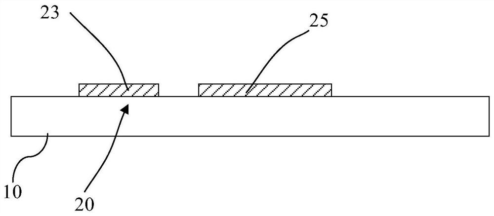
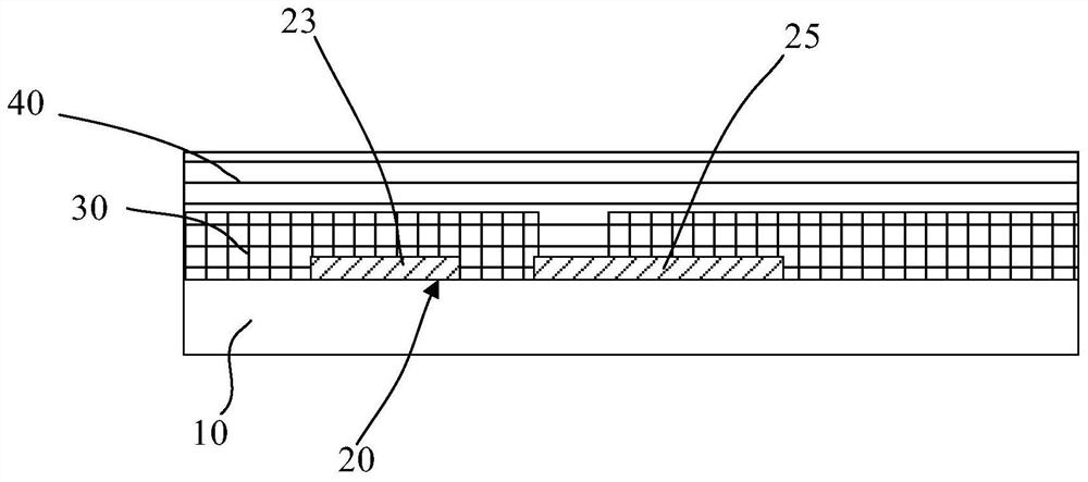
[0031] Please refer to figure 2 , the gate forming step S01 includes depositing and forming a gate (Gate Electrode, GE) layer on the substrate 10 by a physical vapor deposition (Physical Vapor Deposition, PVD) process, and then sequentially applying yellow light to the gate layer 20 process and etching process to pattern the gate layer 20 to form a first gate electrode 23 and a second gate electrode 25 on the gate layer 20 . In a preferred embodiment of the present invention, the gate layer 20 is made of molybdenum (Mo) and / or aluminum (Al). In a preferred embodiment of the present invention, the thickness of the gate layer 20 is 2000-5500 angstroms.

[0032] Please refer to...


PUM

PropertyMeasurementUnit
thicknessaaaaaaaaaa
thicknessaaaaaaaaaa

Abstract

The present invention discloses a manufacturing method of a thin film transistor. The method comprises the steps of: a gate formation step, a semiconductor formation step, an etching termination layerformation step, and a source and drain formation step. The manufacturing method of the thin film transistor performs imaging of the etching termination layer to form an interval portion to separate aswitching thin film transistor and a drive thin film transistor, and a first channel portion and a second channel portion of the switching thin film transistor and the drive thin film transistor areformed by imaging the etching termination layer so that short channel portions are obtained compared to the prior art, and therefore, the thin film transistor easily obtains a short-channel effect.

Description

technical field [0001] The invention relates to a manufacturing method of a thin film transistor device, in particular to a manufacturing method of a thin film transistor device. Background technique [0002] In recent years, oxide semiconductor materials have been widely used in large-scale flat panel displays, especially indium gallium zinc oxide (InGaZnO 4 , IGZO) has attracted widespread attention because of its low-temperature preparation process, low threshold voltage, high mobility, and good large-scale preparation uniformity. In the panel structure of Amorphous Indium Gallium Zinc Oxide (a-IGZO) thin film transistor (Thin Film Transistor, TFT), especially the back channel etching (Back Channel Etched, BCE) structure, due to the (Source) / Drain (Drain) electrode critical dimension loss (Critical Dimension Loss, CD Loss) problem, the width of the channel is limited, how to make a higher resolution thin film transistor panel has become the focus of current development. ...

Claims


Application Information

Patent Timeline
Patent Type & Authority Patents(China)
IPC IPC(8): H01L21/34H01L29/786
Inventor 李金明
Owner TCL CHINA STAR OPTOELECTRONICS TECH CO LTD
Why Eureka
Try Eureka