MOS transistor and method of manufacturing the same

a technology of transistors and transistors, applied in the direction of transistors, semiconductor devices, electrical equipment, etc., can solve the problems of generating floating body effects, affecting the operation so as to improve the operating speed of the device, short channel effect, and reduce the capacitance of the source/drain junction

Inactive Publication Date: 2006-09-21
SAMSUNG ELECTRONICS CO LTD
View PDF17 Cites 0 Cited by
  • Summary
  • Abstract
  • Description
  • Claims
  • Application Information

AI Technical Summary

Benefits of technology

[0018] Furthermore, according to another embodiment of the invention, a gate structure in which a gate insulating layer and a gate electrode are successively stacked is formed on a semiconductor substrate, and then, a first insulating layer is formed on the top and the sides of the gate structure. Second insulating layers are formed on the substrate to be spaced apart from the first insulating layer. An impurity is ion-implanted in the surface portions of the substrate between the gate structure and the second insulating layers, thereby forming lightly doped source / drain regions. Then, heavily doped source / drain regions are formed on the second insulating layers so as to fill gaps between the gate structure and the second insulating layers.
[0019] According to embodiments of the invention, a channel region and the lightly doped source / drain regions (i.e., LDD regions) are formed in the surface of the semiconductor substrate, while the heavily doped source / drain regions are formed on the insulating layer, thereby obtaining the MOS transistor having the similar structure to that of the SOI transistor and performing the same operation as that of a transistor formed on a bulk silicon substrate. So the short channel effect is suppressed and the source / drain junction capacitance is decreased, resulting in the improvement in the operating speed of the device.

Problems solved by technology

In addition to lowering the threshold voltage, a “punchthrough effect” between the source / drain is a severe problem accompanying the short channel effect.
However, as the source / drain junction depth becomes shallower, it becomes more difficult to apply the salicide process.
Therefore, a layer of accumulated holes is formed at the interface in the rear of the SOI layer, thereby generating floating body effects such as parasitic bipolar breakdown, latch-up, etc.

Method used


Image

  • MOS transistor and method of manufacturing the same
  • MOS transistor and method of manufacturing the same
  • MOS transistor and method of manufacturing the same

Examples


Embodiment Construction

[0026] Hereinafter, the preferred embodiments of the invention will be described in detail with reference to the accompanying drawings, where like reference numerals indicate like elements throughout.

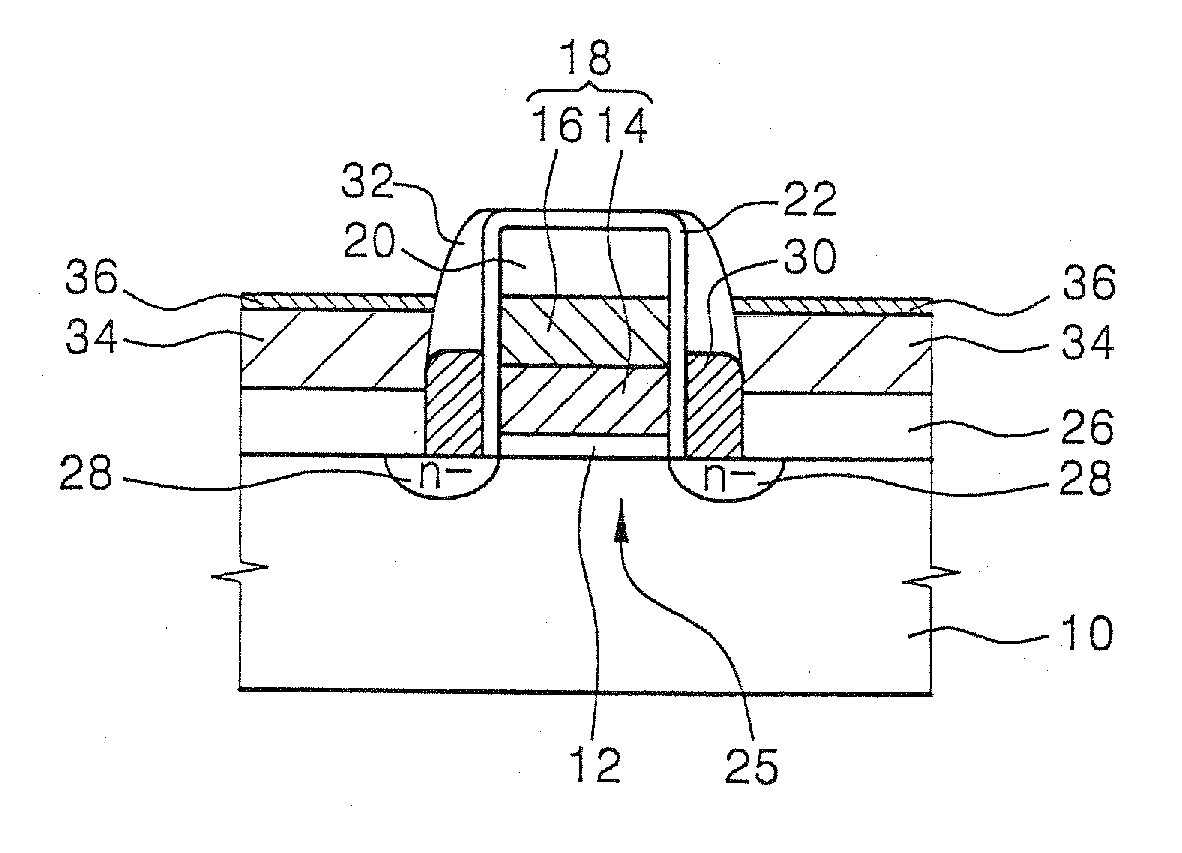
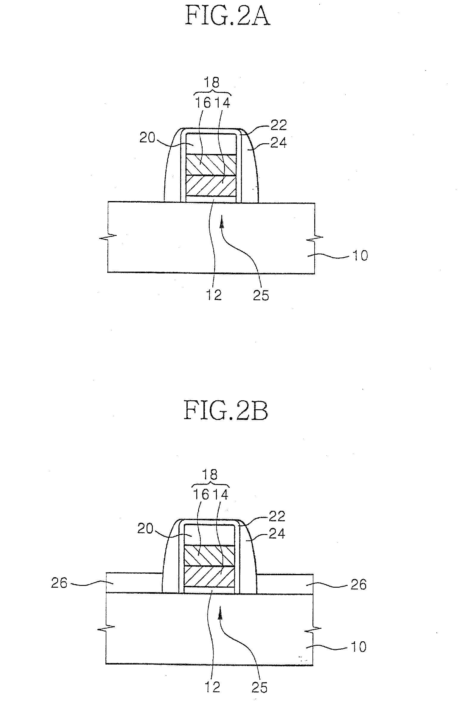
[0027]FIG. 1 is a cross-sectional view of a MOS transistor according to an embodiment of the invention.

[0028] Referring to FIG. 1, a gate structure 25 including a gate insulating layer 12 and a gate electrode 18 is formed on a semiconductor substrate 10. Optionally, the gate structure 25 further includes a gate capping layer 20 formed on the gate electrode 18. The gate capping layer 20 includes an insulating material such as silicon nitride or silicon oxide. In the present embodiment, the gate capping layer 20 is silicon nitride.

[0029] The gate electrode 18 is formed into a polycide structure in which a polysilicon layer 14 and a metal silicide layer 16 are successively stacked.

[0030] A first insulating layer 22 is formed on the top and the sides of the gate structure 25 (that is, t...


PUM


Abstract

In a MOS transistor and a method of manufacturing the same, a gate structure including a gate insulating layer and a gate electrode is formed on a semiconductor substrate. A first insulating layer is formed to cover the gate structure. A second insulating layer is formed on the substrate that is spaced apart from the first insulating layer. A lightly doped source/drain region is formed in the surface portions of the substrate between the second insulating layer and the gate structure. A source/drain extension layer are formed on the lightly doped source/drain region. A heavily doped source/drain region is formed on the second insulating layer so as to connect with the source/drain extension layer. The short channel effect is suppressed and the source/drain junction capacitance is reduced.

Description

CROSS REFERENCE TO RELATED APPLICATIONS [0001] This application is a divisional of U.S. patent application Ser. No. 10 / 440,354, filed on May 15, 2003, now pending, which is claims priority from Korean Patent Application 2002-65649 filed on Oct. 26, 2002, the contents of which are herein incorporated by reference in its entirety.BACKGROUND OF THE INVENTION [0002] 1. Field of the Invention [0003] The invention relates to a semiconductor device and a method of manufacturing the same. More particularly, the invention relates to a semiconductor device capable of suppressing a short channel effect and reducing a source / drain junction capacitance, and a method of manufacturing the same. [0004] 2. Description of the Related Art [0005] As semiconductor devices are developed having a high degree of integration, an active region becomes smaller in size. Thus, a gate length of a MOS transistor formed on the active region becomes shorter. As the gate length decreases, the influence of the source...

Claims


Application Information

Patent Timeline
Patent Type & Authority Applications(United States)
IPC IPC(8): H01L21/8242H01L21/336H01L21/28H01L21/8234H01L27/088H01L29/417H01L29/423H01L29/49H01L29/78
CPCH01L29/41775H01L29/41783H01L29/66628Y10S257/90H01L29/78
Inventor LEE, JAE-KYU
Owner SAMSUNG ELECTRONICS CO LTD
Why Eureka
Try Eureka