
N-type mosfet

a mosfet and n-type technology, applied in the field of n-type mosfet, can solve the problems of increasing the short channel effect (sce) of a mosfet having planar transistor structure, increasing the instability of the sip epitaxial layer,

Pending Publication Date: 2022-08-25
SHANGHAI HUALI INTEGRATED CIRCUIT CORP
View PDF0 Cites 0 Cited by
  • Summary
  • Abstract
  • Description
  • Claims
  • Application Information

AI Technical Summary

Benefits of technology

The present patent provides an N-type MOSFET that can mitigate the short channel effect, which improves the performance of transistors. This is achieved by improving the structure of the embedded epitaxial layer, which helps to prevent deterioration of the short channel effect when the length of the gate structure is reduced to less than 20 nm at a process node below 7 nm. By using a SiAs epitaxial layer or a structure formed by superposing a SiP epitaxial layer on the surface of a SiAs epitaxial layer, the short channel effect can be significantly improved, resulting in improved carrier mobility and better performance of the device.

Problems solved by technology

As the semiconductor process technology keeps on reducing target dimensions with each roadmap node, short channel effect (SCE) of a MOSFET having planar transistor structures has become increasingly significant and problematic.
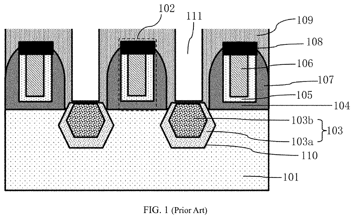
However, the phosphorus (P) in the SiP epitaxial layer 103 diffuse easily, causing instability of the SiP epitaxial layer.

Method used


Image

  • N-type mosfet
  • N-type mosfet

Examples


first embodiment

N-Type MOSFET of the First Embodiment

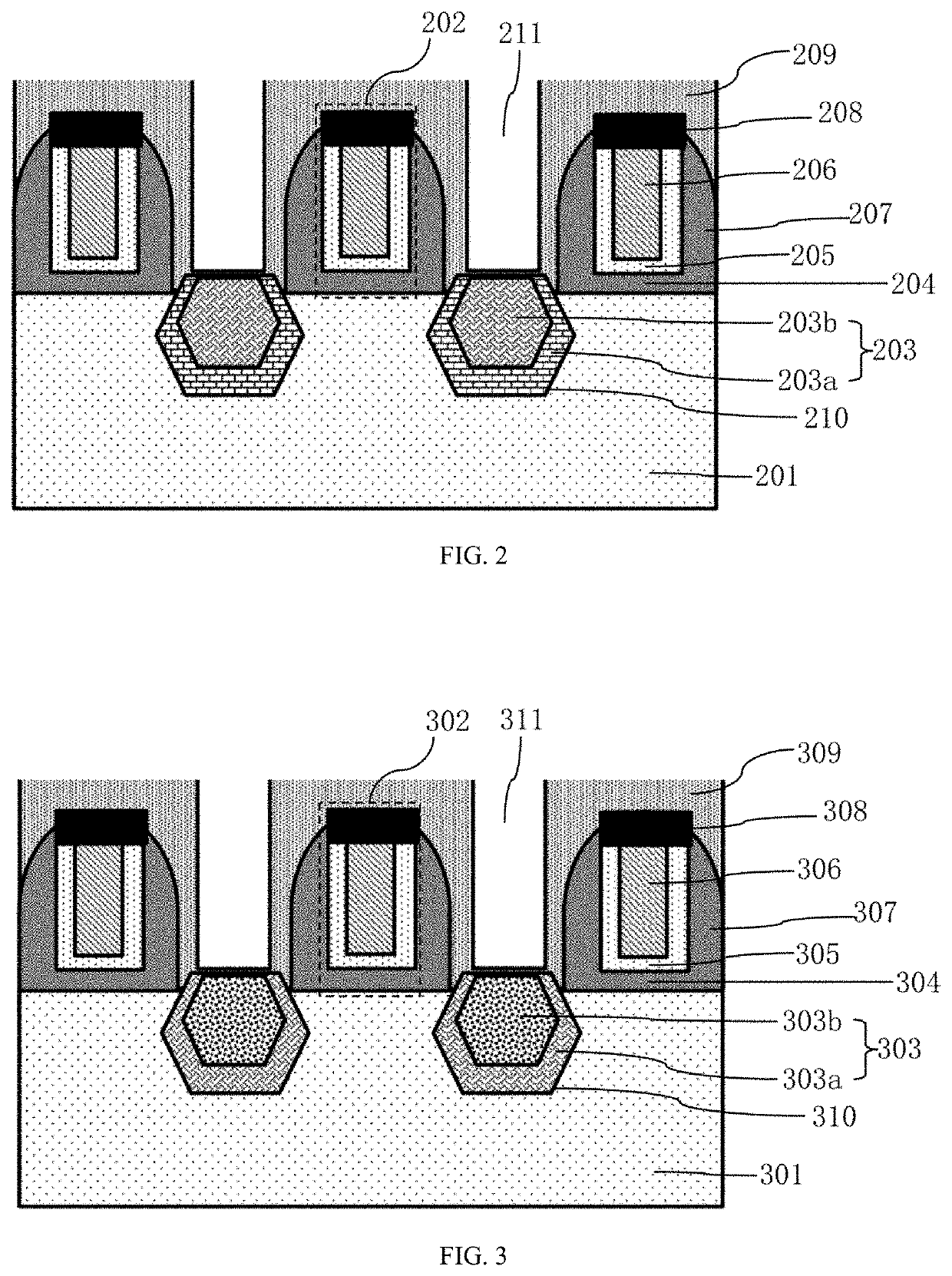
[0038]FIG. 2 shows a schematic cross section of a structure of an N-type MOSFET according to the first embodiment of the present disclosure. The N-type MOSFET includes:

[0039]a gate structure formed on the surface of a semiconductor substrate 201, here the gate structure is shown in the dashed line box 202.

[0040]An embedded epitaxial layer 203 is formed on each side of the gate structure, the embedded epitaxial layer 203 fills in a groove 210, and the groove 210 is formed in the semiconductor substrate 201.

[0041]The semiconductor substrate 201 includes a silicon substrate.

[0042]The groove 210 is Σ-shaped. The groove 210 is generally formed by dry etching for some time and wet etching for some time. Silicon's three crystal orientations (100), (010) and (111) have different etching rates during wet etching process, resulting in the Σ-shaped structure.

[0043]The Σ-shaped embedded epitaxial layer 203 are arranged to be a source region and a drain regio...

second embodiment

N-Type MOSFET of the Second Embodiment

[0059]FIG. 3 is a schematic cross section of a structure of an N-type MOSFET, according to the second embodiment of the present disclosure. The N-type MOSFET of the second embodiment includes:

[0060]a gate structure formed on the surface of a semiconductor substrate 301, the gate structure is shown in the dashed line box 302.

[0061]An embedded epitaxial layer 303 is formed on each side of the gate structure, the embedded epitaxial layer 303 fills in a groove 310, and the groove 310 is formed in the semiconductor substrate 301.

[0062]The semiconductor substrate 301 includes a silicon substrate.

[0063]The groove 310 is Σ-shaped. The groove 310 is generally formed by dry etching for some time and wet etching for some time. Silicon's three crystal orientations (100), (010) and (111) have different etching rates during wet etching process, resulting in the Σ-shaped structure.

[0064]A source region and a drain region are formed in the embedded epitaxial la...


PUM


Abstract

The present application discloses an N-type MOSFET, comprising: a gate structure formed on the surface of a semiconductor substrate; an embedded epitaxial layer formed on each of the two sides of the gate structure, wherein the embedded epitaxial layer fills in a groove, and the groove is formed in the semiconductor substrate; and a source region and a drain region formed in the embedded epitaxial layer on each side of the gate structure; wherein the width of the gate structure is less than 20 nm; and the embedded epitaxial layer comprises a first epitaxial layer of SiAs, or the embedded epitaxial layer is formed by stacking a second epitaxial layer of SiAs and a third epitaxial layer of SiP. The present application can improve the carrier mobility of the device and improve the short channel effect.

Description

CROSS-REFERENCES TO RELATED APPLICATIONS[0001]This application claims the priority to Chinese patent application No. CN202110196849.0, filed on Feb. 22, 2021, and entitled “N-TYPE MOSFET”, the disclosure of which is incorporated herein by reference in entirety.TECHNICAL FIELD[0002]The present application relates a semiconductor integrated circuit, in particular, to an N-type MOSFET.BACKGROUND[0003]As the semiconductor process technology keeps on reducing target dimensions with each roadmap node, short channel effect (SCE) of a MOSFET having planar transistor structures has become increasingly significant and problematic. At the devices dimension reach under 20 nm, fin field-effect transistors (FinFETs) have been proven effective. The FinFETs have three-dimensional structures, there gate structures cover the top surfaces and side surfaces of fins, and a channel is formed on the top surface and two side surfaces of each fin, thus the ability of the gate structure to mediate between th...

Claims


Application Information

Patent Timeline
IPC IPC(8): H01L29/08H01L29/78H01L29/423H01L29/06H01L29/267
CPCH01L29/0847H01L29/785H01L29/42392H01L29/0669H01L29/267H01L29/78B82Y10/00H01L29/775H01L29/0673
Inventor WENG, WENYIN
Owner SHANGHAI HUALI INTEGRATED CIRCUIT CORP
Learn More