Semiconductor device and a method of manufacturing the same, and solid-state image pickup device using the same

a semiconductor and pickup device technology, applied in the direction of semiconductor devices, radio frequency controlled devices, electrical apparatus, etc., can solve the problems of reducing promoting the high performance peak, and deteriorating the character of the mutual conductance gm, so as to improve the gain of the source follower circuit, promote the high performance and promote the effect of the mos transistor

Inactive Publication Date: 2014-08-28
SONY CORP
View PDF0 Cites 1 Cited by
  • Summary
  • Abstract
  • Description
  • Claims
  • Application Information

AI Technical Summary

Benefits of technology

[0013]The embodiments of the present invention have been made in order to solve the problem described above, and it is therefore desirable to provide a semiconductor device in which reduction in mutual conductance (hereinafter referred to as “gm” for short) is suppressed, and a mutual conductance between a source and a drain (hereinafter referred to as “gds” for short) and a mutual conductance of a back gate (hereinafter referred to as “gmb” for short) are maintained, thereby making promotion of a high performance of a MOS transistor possible and a method of manufacturing the same, and a solid-state image pickup device using the same.
[0015]In the semiconductor device according to the embodiment of the present invention, the hot carrier current is suppressed by the LDD region, the short channel effect is suppressed by the extension region, and gds between the source region and the drain region is improved. In addition, a channel region can be formed lightly in impurity concentration and thus gm is prevented from being made worse because the short channel effect is suppressed. In addition, since the extension region can be formed at the higher impurity concentration than that of the LDD region, the parasitic resistance is hardly increased, and thus the reduction in gm is less.
[0017]In the method of manufacturing a semiconductor device according to another embodiment of the present invention, the hot carrier current is suppressed by forming the LDD region, the short channel effect is suppressed by forming the extension region, and gds between the source region and the drain region is improved. In addition, a channel region can be formed lightly in impurity concentration and gm is prevented from being made worse because the short channel effect is suppressed. In addition, since the extension region can be formed at the higher impurity concentration than that of the LDD region, the parasitic resistance is hardly increased, and thus the reduction in gm is less.
[0020]According to the semiconductor device of the embodiments of the present invention, there is obtained an advantage that the high performance of the MOS transistor can be promoted because the reduction in gm showing the trade-off relationship with gds and gmb can be suppressed, and thus gds and gmb can be maintained. Therefore, using the semiconductor device of the embodiments of the present invention in the source follower circuit makes it possible to improve the gain of the source follower circuit.
[0021]According to the method of manufacturing a semiconductor device of the embodiments of the present invention, there is obtained an advantage that the high performance of the MOS transistor can be promoted because the reduction in gm showing the trade-off relationship with gds and gmb can be suppressed, and thus gds and gmb can be maintained. Therefore, using the semiconductor device of the embodiments of the present invention in the source follower circuit makes it possible to improve the gain of the source follower circuit.
[0022]According to the solid-state image pickup device of the embodiments of the present invention, there is obtained an advantage that the high performance of the output circuit can be promoted because the high-performance MOS transistor can be used in the source follower circuit, and thus the gain of the source follower circuit can be improved.

Problems solved by technology

However, with the LDD structure described above, a large parasitic resistance is generated and thus the characteristics of the mutual conductance gm is deteriorated because diffusion layer such as a source region and a drain region are each formed at a low impurity concentration.
However, the asymmetrical deep diffusion layer structure on the source side is not introduced to the devices so much because the improvement in the gain of the source follower circuit may not be obtained as expected.
That is to say, the reason for this is because the mutual conductance gds between the source and the drain is made worse, thereby reducing the gain of the source follower circuit.
As a result, the promotion of the high performance peaks out, which becomes a problem.

Method used


Image

  • Semiconductor device and a method of manufacturing the same, and solid-state image pickup device using the same
  • Semiconductor device and a method of manufacturing the same, and solid-state image pickup device using the same
  • Semiconductor device and a method of manufacturing the same, and solid-state image pickup device using the same

Examples


first embodiment

1. First Embodiment

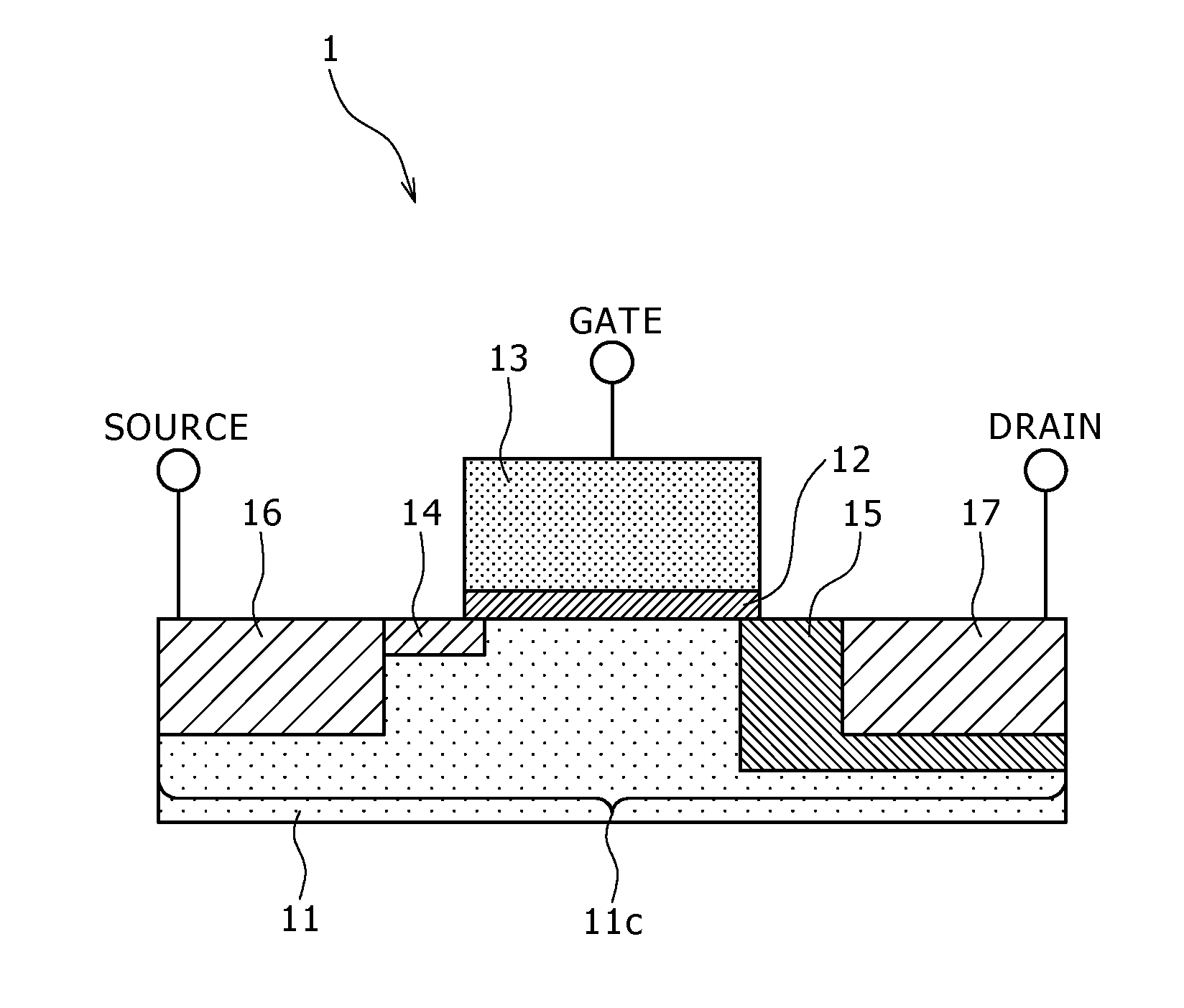
[0033]A semiconductor device according to a first embodiment of the present invention includes: a gate electrode formed on a semiconductor substrate through a gate insulating film; an extension region formed in the semiconductor substrate on a source side of the gate electrode; a source region formed in the semiconductor substrate on the source side of the gate electrode through the extension region; an LDD region formed in the semiconductor substrate on a drain side of the gate electrode; and a drain region formed in the semiconductor substrate on the drain side of the gate electrode through the LDD region; in which the extension region is formed at a higher concentration than that of the LDD region so as to be shallower than the LDD region.

First Example

[0034]A first example of the semiconductor device according to the first embodiment of the present invention will be described in detail hereinafter with reference to a schematic structural cross sectional view of...

second embodiment

2. Second Embodiment

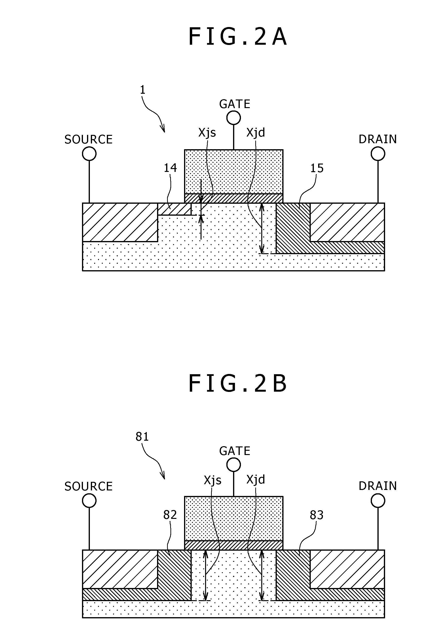
[0106]A method of manufacturing the semiconductor device according to a second embodiment of the present invention includes the steps of: forming the gate electrode on the semiconductor substrate through the gate insulating film; forming the LDD region in the semiconductor substrate on the drain side of the gate electrode; forming the extension region in the semiconductor substrate on the source side of the gate electrode; forming the source region in the semiconductor substrate on the source side of the gate electrode through the extension region, and forming the drain region in the semiconductor substrate on the drain side of the gate electrode through the LDD region; and forming the extension region at a higher impurity concentration than that of the LDD region so as to be shallower than the LDD region.

first example

[0107]A first example of the method of manufacturing the semiconductor device according to the second embodiment of the present invention will be described in detail hereinafter with reference to cross sectional views showing respective manufacturing processes of FIGS. 6A to 6F.

[0108]As shown in FIG. 6A, channel ion implantation for formation of the channel region 11c is carried out for the semiconductor substrate 11. The silicon semiconductor substrate, for example, is used as the semiconductor substrate 11. Alternatively, the SOI substrate or the like may be used as the semiconductor substrate 11.

[0109]In the case of the NMOS transistor, in the channel ion implantation process, either boron or indium ions are implanted into the semiconductor substrate 11. When the boron ions are implanted into the semiconductor substrate 11, an implantation energy is set in the range of 3 to 100 keV, and a dosage is set at 5×10¹³ / cm2 or less. On the other hand, when the indium ions are implanted i...


PUM


Abstract

A semiconductor device, including: a gate electrode formed on a semiconductor substrate through a gate insulating film; an extension region formed in the semiconductor substrate on a source side of the gate electrode; a source region formed in the semiconductor substrate on the source side of the gate electrode through the extension region; an LDD region formed in the semiconductor substrate on a drain side of the gate electrode; and a drain region formed in the semiconductor substrate on the drain side of the gate electrode through the LDD region; wherein the extension region is formed at a higher concentration than that of the LDD region so as to be shallower than the LDD region.

Description

RELATED APPLICATION DATA[0001]This application is a division of U.S. patent application Ser. No. 12 / 604,508 filed Oct. 23, 2009, the entirety of which is incorporated herein by reference to the extent permitted by law. The present application claims the benefit of priority to Japanese Patent Application No. JP 2008-279474 filed on Oct. 30, 2008 in the Japan Patent Office, the entirety of which is incorporated by reference herein to the extent permitted by law.BACKGROUND OF THE INVENTION[0002]1. Field of the Invention[0003]The present invention relates to a semiconductor device and a method of manufacturing the same, and a solid-state image pickup device using the same.[0004]2. Description of the Related Art[0005]A source follower circuit used in an output portion of a solid-state image pickup element is a circuit for amplifying a resulting signal from a pixel, and driving a load in a subsequent stage. In general, a CMOS (Complementary Metal Oxide Semiconductor) transistor is used in...

Claims


Application Information

Patent Timeline
Patent Type & Authority Applications(United States)
IPC IPC(8): H01L29/78H01L27/146H01L29/66H01L21/336H01L29/786
CPCH01L29/7835H01L29/66492H01L27/14612H01L21/26513H01L27/1461H01L27/14689H01L29/0847H01L29/66659H01L29/78624H01L29/42312
Inventor NAKAMURA, RYOSUKE
Owner SONY CORP
Why Eureka
Try Eureka