Display panel and display device

A display panel and substrate layer technology, applied to electrical components, electrical solid devices, circuits, etc., can solve the problems of low light transmittance and large opening diameter of panel stacking, and achieve improved light transmittance and high screen-to-body ratio , the effect of reducing the diameter

Inactive Publication Date: 2019-06-07
WUHAN CHINA STAR OPTOELECTRONICS SEMICON DISPLAY TECH CO LTD
View PDF6 Cites 38 Cited by
  • Summary
  • Abstract
  • Description
  • Claims
  • Application Information

AI Technical Summary

Problems solved by technology

[0005] An object of the present invention is to provide a display panel, which can solve the problems of low light transmittance and excessively large opening diameter in panel stacking in the prior art.

Method used


Image

  • Display panel and display device
  • Display panel and display device
  • Display panel and display device

Examples


Embodiment 1

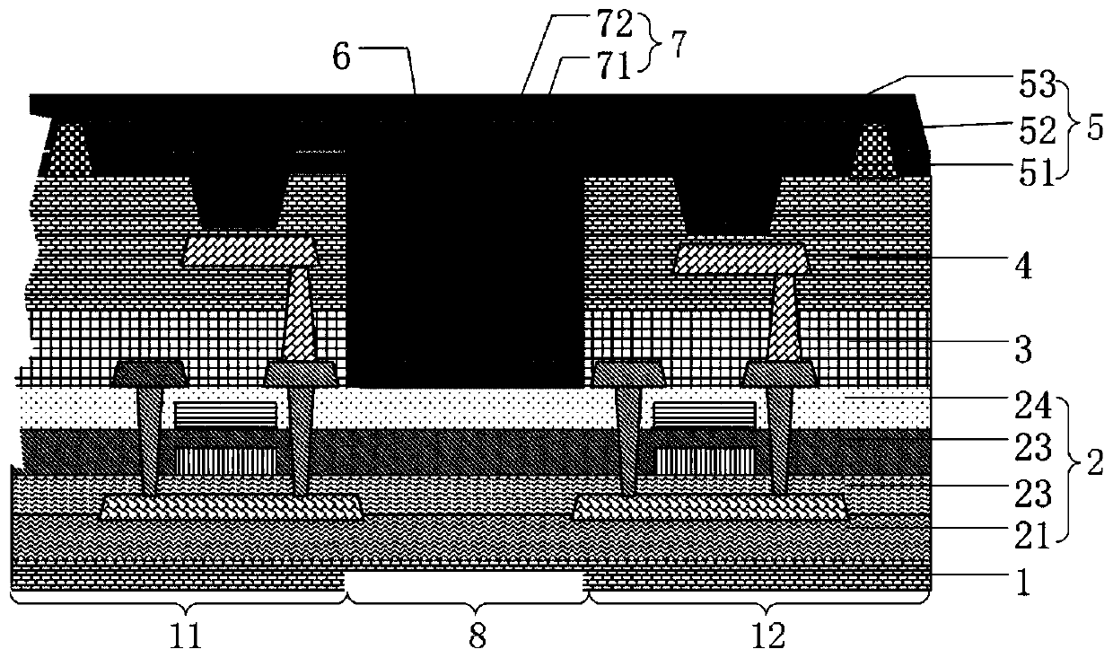
[0026] see figure 1 , figure 1 The schematic cross-sectional view of the display panel provided in this embodiment, in order to achieve the above purpose, the present invention provides a display panel, including a substrate layer 1, a thin film transistor layer 2, a flat layer 3, a pixel definition layer 4 and a thin film encapsulation layer arranged in sequence Layer 5.

[0027] The substrate layer 1 is a PI film layer, that is, a polyimide film, which is used as the base of the display panel; the polyimide film is a thin film insulating material with better performance in the world, and has a strong tensile strength. It is formed by polycondensation of pyromellitic dianhydride and diaminodiphenyl ether in a strong polar solvent, casting into a film and then imidization.

[0028] The thin film transistor layer 2 includes a buffer layer 21, a first gate insulating layer 22, a second gate insulating layer 23 and a barrier layer 24; wherein the buffer layer 21 is arranged on ...

Embodiment 2

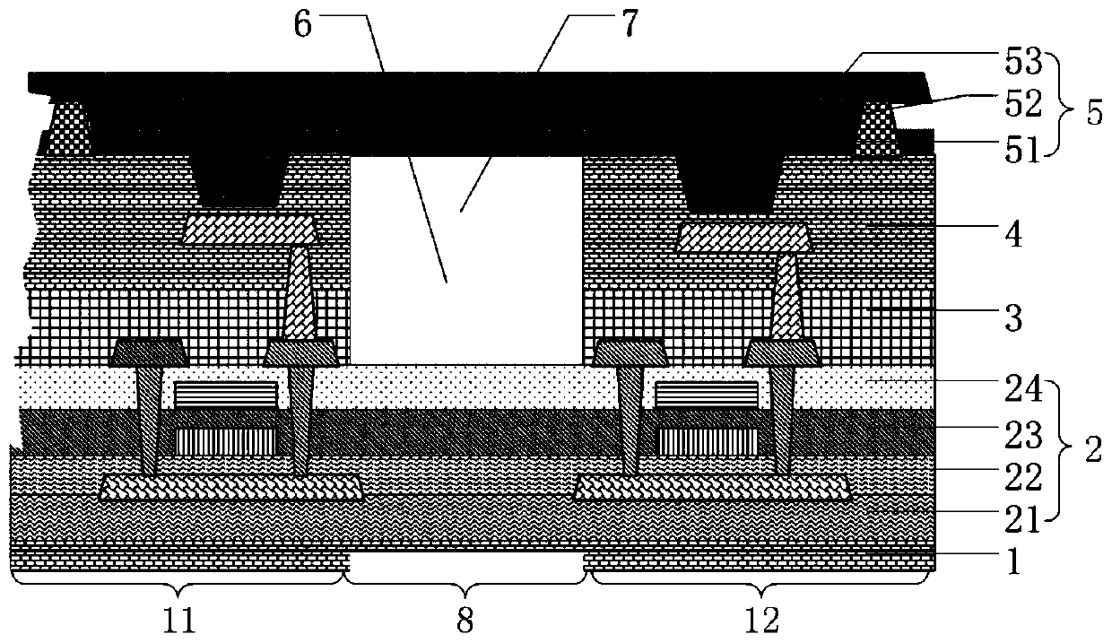
[0036] see image 3 , image 3 Shown is a schematic cross-sectional view of the display panel provided by this embodiment. The structure of the transparent display panel in this embodiment is roughly the same as that of Embodiment 1. For the same structure, refer to the above method, which will not be repeated here. The main differences are The reason is that the material of the filling layer 7 is a transparent organic material, and its light transmittance is greater than that of the pixel definition layer 4 and the flat layer 3. Therefore, such an arrangement improves the light transmittance to a certain extent, and can further reduce the light transmittance. The small opening diameter achieves a high screen-to-body ratio.

Embodiment 3

[0038] see Figure 4 , Figure 4Shown is a schematic cross-sectional view of the display panel provided by this embodiment. The structure of the transparent display panel in this embodiment is roughly the same as that of Embodiment 1. For the same structure, refer to the above method, which will not be repeated here. The main differences are The reason is that the cross-sectional shape of the via hole 6 is an inverted trapezoid, and the side wall of the via hole 6 forms an obtuse angle with its bottom surface. As the angle increases, the film thickness evaporated on the side increases. When the formed angle is greater than 120 degrees, the sidewall of the via hole 6 cannot reflect. Therefore, when the angle between the side wall of the via hole 6 and its bottom surface is controlled to be greater than 90 degrees and less than 120 degrees, the side wall of the via hole 6 can serve as a reflector to reflect light, so that more electronic components placed under the groove 8 can...


PUM


Abstract

The invention provides a display panel and a display device. The display panel comprises a substrate layer, a film transistor layer, a flat layer, a pixel definition layer and a film package layer which are arranged sequentially; and first pixels and second pixels which are arranged in a mutually spaced mode are formed on the pixel definition layer, wherein passing holes are formed in the positions, between the first pixels and the second pixels, of the pixel definition layer and the flat layer, and the passing holes are filled with filling layers. The display panel and the display device havethe advantages that the light transmittance of a camera module below a substrate is improved, the diameter of the passing holes is decreased, and the purpose of the high screen ratio is achieved.

Description

technical field [0001] The present invention relates to the technical field of display panels, in particular to a display panel and a display device. Background technique [0002] In the past two years, the full screen market has developed rapidly in the market. Among them, notch screens and water drop screens have gradually occupied the mainstream of the market. The main feature is the pursuit of a higher screen-to-body ratio. At present, there are voices of a higher screen-to-body ratio in the market. Although there are no real mass products on the market, various companies are already developing them. Its development idea is to design holes on the screen, place the front camera, and hide the camera module in the panel. In order to ensure that the camera module can receive more light, the light transmittance of the panel stack must be greatly improved. high demands. [0003] Since the camera module is under the PI (Polyimide Film, polyimide) film layer, and the PI materi...

Claims


Application Information

Patent Timeline
Patent Type & Authority Applications(China)
IPC IPC(8): H01L27/32
CPCH10K59/124H10K59/122H10K59/8731H10K50/844
Inventor 郑敏欧阳齐周阳
Owner WUHAN CHINA STAR OPTOELECTRONICS SEMICON DISPLAY TECH CO LTD
Why Eureka
Try Eureka