On-chip integrated cascade amplification semiconductor laser

A cascade amplification, laser technology, applied in the direction of semiconductor lasers, lasers, laser parts, etc., to achieve the effect of preventing deterioration, improving output power, and improving laser brightness

Active Publication Date: 2019-06-11
INST OF APPLIED ELECTRONICS CHINA ACAD OF ENG PHYSICS
View PDF2 Cites 6 Cited by
  • Summary
  • Abstract
  • Description
  • Claims
  • Application Information

AI Technical Summary

Problems solved by technology

Affected by cavity surface damage, nonlinear effects, etc., the current maximum output power of 100μm wide chips is limited to about 30W. To continue to increase output power, it is urgent to carry out innovative research on chip design.

Method used


Image

  • On-chip integrated cascade amplification semiconductor laser
  • On-chip integrated cascade amplification semiconductor laser
  • On-chip integrated cascade amplification semiconductor laser

Examples


Embodiment Construction

[0033] All features disclosed in this specification, or steps in all methods or processes disclosed, may be combined in any manner, except for mutually exclusive features and / or steps.

[0034] Any feature disclosed in this specification (including any appended claims, abstract), unless otherwise stated, may be replaced by alternative features which are equivalent or serve a similar purpose. That is, unless expressly stated otherwise, each feature is one example only of a series of equivalent or similar features.

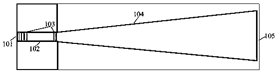
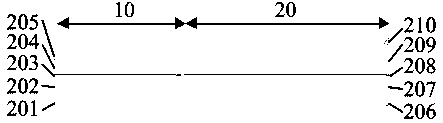
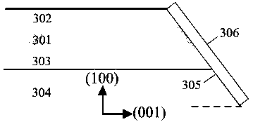
[0035] Such as image 3 and 4 As shown, this embodiment discloses an on-chip integrated cascade amplifier semiconductor laser, which includes a ridge region 10, an on-chip DBR (distributed Bragg reflector, distributed Bragg reflector) grating structure 103, a tapered region 20 and a step thick epitaxial waveguide; the DBR grating structure 103 is arranged on the ridge-shaped region 10; the ridge-shaped region 10 is a ridge-shaped waveguide structure, and the taper...


PUM


Abstract

The invention discloses an on-chip integrated cascade amplification semiconductor laser. The on-chip integrated cascade amplification semiconductor laser comprises a ridge type area, an on-chip DBR grating structure, a tapered type area and an epitaxial waveguide; the DBR grating structure is arranged on the ridge type area, the ridge type area is a ridge type waveguide structure, the tapered typearea is a gain waveguide structure; the epitaxial waveguide has a first-order ladder thickness; the ridge type area is arranged at a thin side of the epitaxial waveguide, the tapered type area is arranged at a thick side of the epitaxial waveguide, and the ridge type area and the tapered type area are cascaded. The laser of the design can more sufficiently utilize the tapered type area gain in comparison with a laser amplification way of traditionally utilizing the tapered gain structure; the base model feature is maintained when the mode volume is extended based on the iso-luminous flux principle, the optical quality of the near diffraction limit laser is guaranteed, and the brightness is greatly improved.

Description

technical field [0001] The invention relates to the field of semiconductor lasers, in particular to an on-chip integrated cascaded amplifier semiconductor laser. Background technique [0002] With the innovation of technology, high-power semiconductor laser chip (LD) develops rapidly, and it has been widely used as a pump light source in civil and military fields. Especially in recent years, its development momentum as a fiber laser pump source is extremely rapid. As fiber lasers continue to increase the output brightness requirements of semiconductor laser pump sources, the number of traditional pigtail pump source coupled semiconductor laser chips is close to the physical limit, and continuing to increase the output brightness can only increase the brightness of the chip. In addition, realizing direct output of high-brightness semiconductor lasers through high-quality and high-efficiency common-aperture beam combining is also one of the important ways to study a new gener...

Claims


Application Information

Patent Timeline
Patent Type & Authority Applications(China)
IPC IPC(8): H01S5/125H01S5/22H01S5/042
Inventor 唐淳周坤杜维川康俊杰李弋谭昊王昭高松信
Owner INST OF APPLIED ELECTRONICS CHINA ACAD OF ENG PHYSICS
Why Eureka
Try Eureka