Method for manufacturing element structure

A manufacturing method and structure technology, which are applied in the manufacture of semiconductor/solid-state devices, electrical components, and electrical solid-state devices, etc., can solve the problems of poor coverage, difficulty in ensuring barrier properties, and low coverage characteristics, and improve sealing performance. , Prevent the decline of barrier properties and improve the effect of barrier properties

Active Publication Date: 2019-06-14
ULVAC INC
View PDF10 Cites 0 Cited by
  • Summary
  • Abstract
  • Description
  • Claims
  • Application Information

AI Technical Summary

Problems solved by technology

[0005] However, the coverage characteristics (step (step difference) coverage) of inorganic films that have barrier properties to water vapor and the like are relatively low, and if there are irregularities on the surface of the substrate with the device layer, the inorganic films cannot sufficiently cover the irregularities.
For example, poor coverage may occur where the boundary of the unevenness formed on the substrate surface is not covered by the inorganic film.
If such poor coverage of the inorganic film occurs, it will be difficult to ensure sufficient barrier properties because moisture intrusion from the part where the poor coverage occurs cannot be prevented.

Method used


Image

  • Method for manufacturing element structure
  • Method for manufacturing element structure
  • Method for manufacturing element structure

Examples


Embodiment Construction

[0033] Next, an apparatus for manufacturing the element structure according to the first embodiment of the present invention will be described based on the drawings.

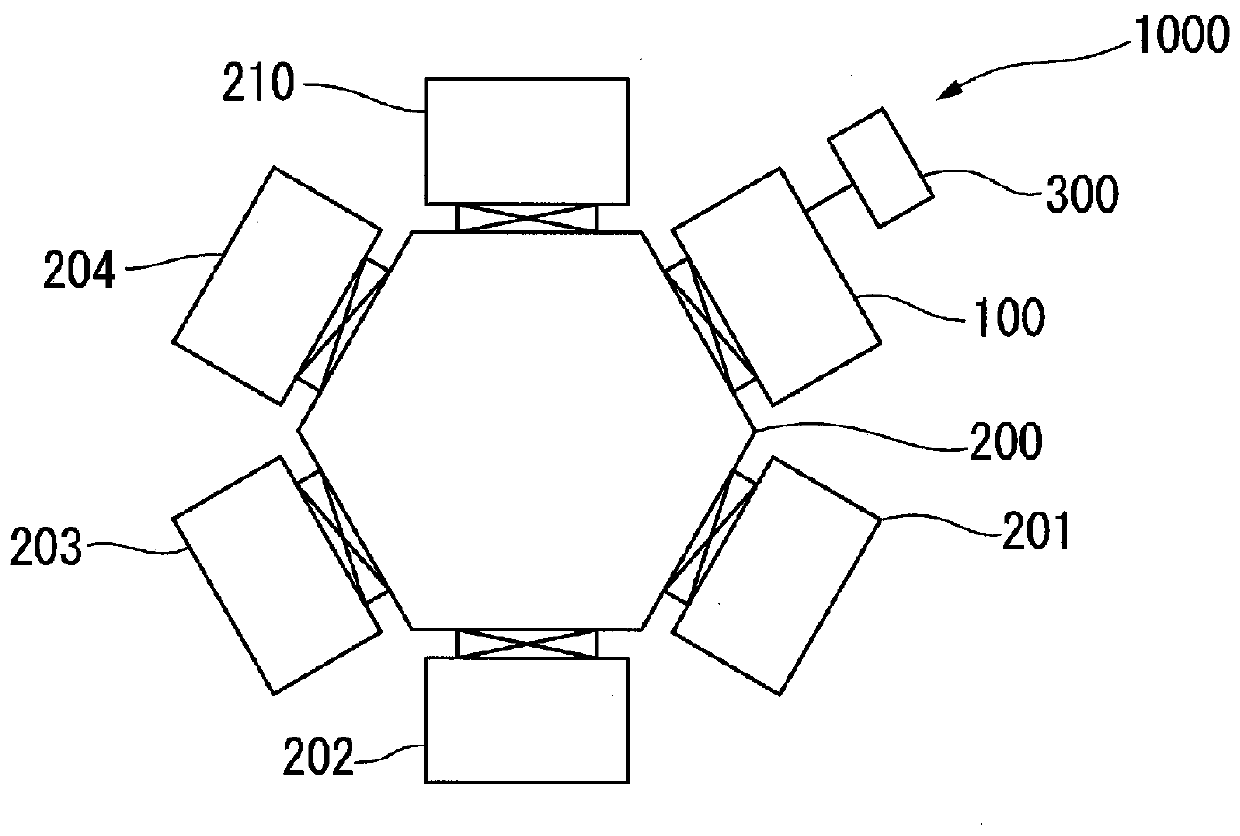
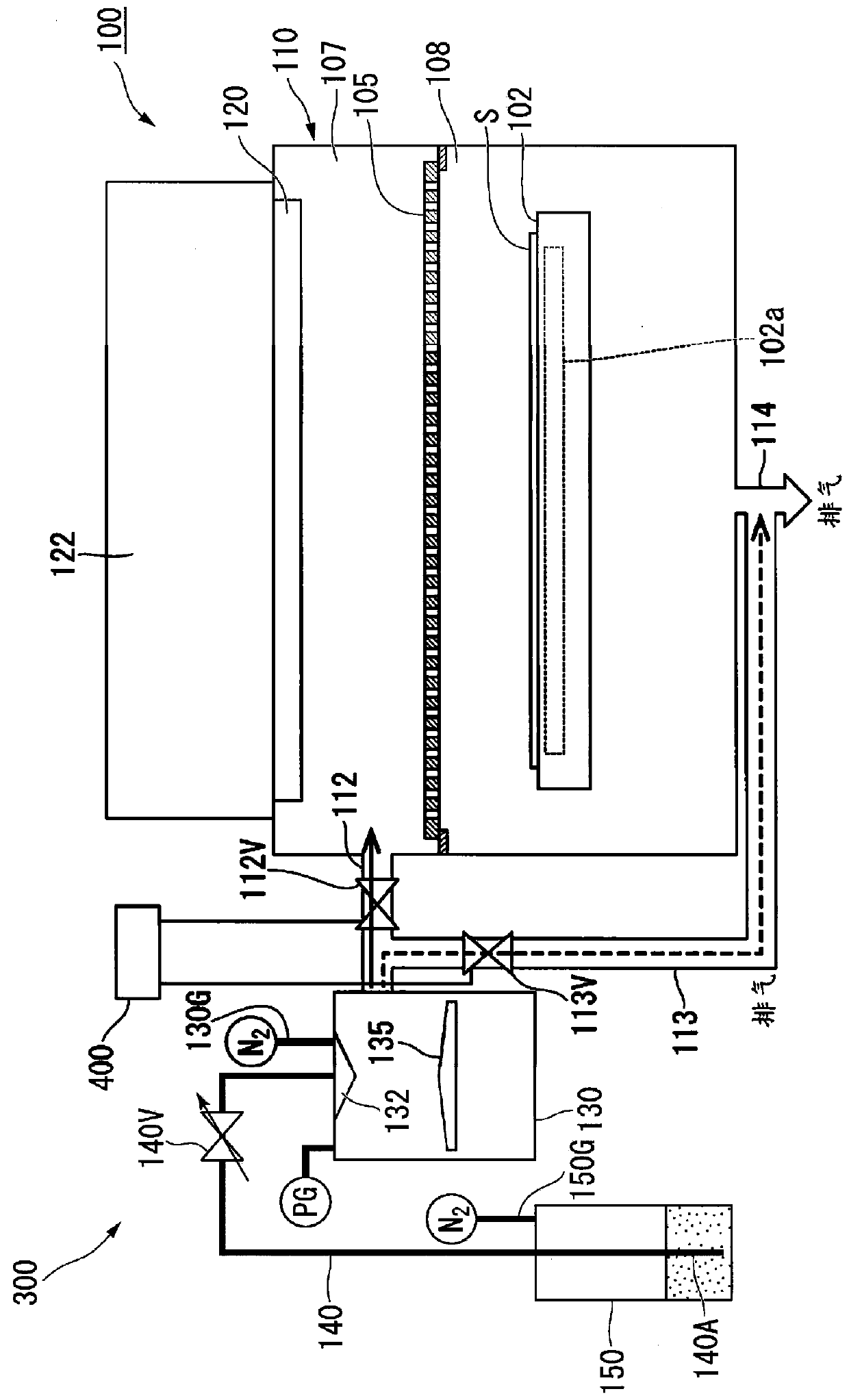
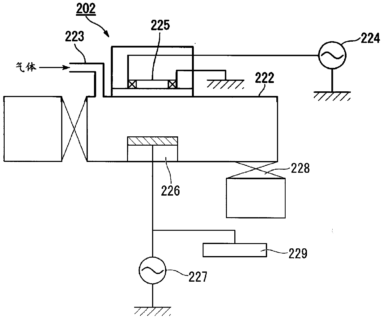
[0034] figure 1 It is a schematic diagram which shows the manufacturing apparatus in the manufacturing method of the element structure which concerns on this embodiment. figure 2 It is a schematic diagram which shows the resin film-forming part which concerns on this embodiment. image 3 is a schematic diagram showing a partial presence processing unit of the device for manufacturing the element structure according to the present embodiment, and is shown in figure 1 Among them, the reference numeral 1000 is a manufacturing apparatus of an element structure.

[0035] As will be described later, the device 1000 for producing an element structure according to the present embodiment produces an element structure such as an organic EL element. like figure 1 As shown, the manufacturing apparatus 1000 includes a f...


PUM


Abstract

A method for manufacturing an element structure according to the present invention comprises: a resin material formation step for forming a resin material comprising an organic compound on an uneven substrate so that at least an area around a protruding part is thicker than a flat part; and a resin material etching step for removing the resin material at the flat part while leaving part of the resin material located around the protruding part. In the resin material etching step, a change in a specific condition among conditions for performing an etching process on the resin material is detected, and the detected detection result is used as the end point of the etching process.

Description

technical field [0001] The present invention relates to a method for manufacturing an element structure having a laminated structure that protects devices and the like from oxygen, moisture, etc. . [0002] This application claims priority based on Patent Application No. 2017-030316 filed in Japan on February 21, 2017, the contents of which are incorporated herein by reference. Background technique [0003] An organic EL (Electro Luminescence) element etc. are known as an element which contains the compound which has the property which is easily deteriorated by moisture, oxygen, etc., for example. With regard to such an element, an attempt has been made to suppress the intrusion of moisture and the like into the element by forming a laminated structure in which a layer containing a compound and a protective layer covering the layer are laminated. For example, Patent Document 1 below describes a light-emitting element having a protective film formed of a laminated film of a...

Claims


Application Information

Patent Timeline
Patent Type & Authority Applications(China)
IPC IPC(8): H05B33/10H01L21/3065H01L51/50H05B33/04
CPCH01L21/3065H05B33/04H05B33/10H10K50/00H01L21/31116H10K71/00
Inventor 清健介青代信高桥明久矢岛贵浩加藤裕子
Owner ULVAC INC
Why Eureka
Try Eureka