A chopper amplification circuit adopting a negative impedance compensation technology

A technology of amplifying circuits and negative impedance, which is applied in the field of analog circuit design, can solve problems such as high input impedance, boost, and affect circuit stability, and achieve high input impedance, expand application prospects, and high stability.

Active Publication Date: 2019-06-21
SOUTH CHINA UNIV OF TECH
View PDF7 Cites 8 Cited by
  • Summary
  • Abstract
  • Description
  • Claims
  • Application Information

AI Technical Summary

Problems solved by technology

However, using this method, when the amount of positive feedback introduced is too large, it will affect the stability of the circuit, and it is difficult to increase the input impedance to a level above GΩ, which cannot meet some applications that require extremely high input impedance.
That is, the chopper amplifier circuit in the prior art cannot be applied to some occasions that require extremely high input impedance

Method used


Image

  • A chopper amplification circuit adopting a negative impedance compensation technology
  • A chopper amplification circuit adopting a negative impedance compensation technology
  • A chopper amplification circuit adopting a negative impedance compensation technology

Examples


Embodiment 1

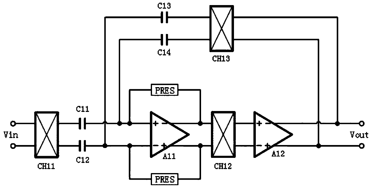
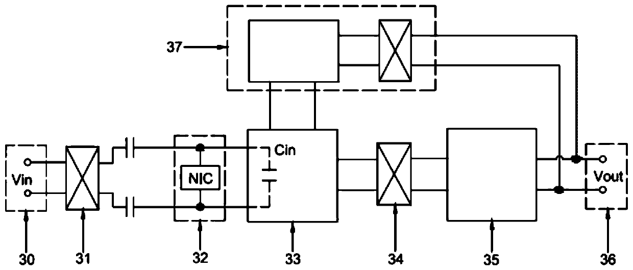
[0053] Such as Figure 5 As shown, the first-stage amplifying circuit 33 includes a third operational amplifier A3, a third pseudo-resistor R3, a fourth pseudo-resistor R4, a fifth pseudo-resistor R5, and a sixth pseudo-resistor R6; the third operational amplifier A3 includes a corresponding first non-inverting input terminal and a first inverting input terminal, a corresponding second non-inverting input terminal and a second inverting input terminal, and also includes a positive output terminal and a negative output terminal; the first One of the output terminals of the stage chopping switch 31 is connected to the first inverting input terminal through the input capacitor, and the second output terminal is connected to the second non-inverting input terminal through the input capacitor, and the positive output terminal is passed through the first inverting input terminal in turn. The second-stage chopper switch 34, the second-stage amplifying circuit 35 and the negative feed...

Embodiment 2

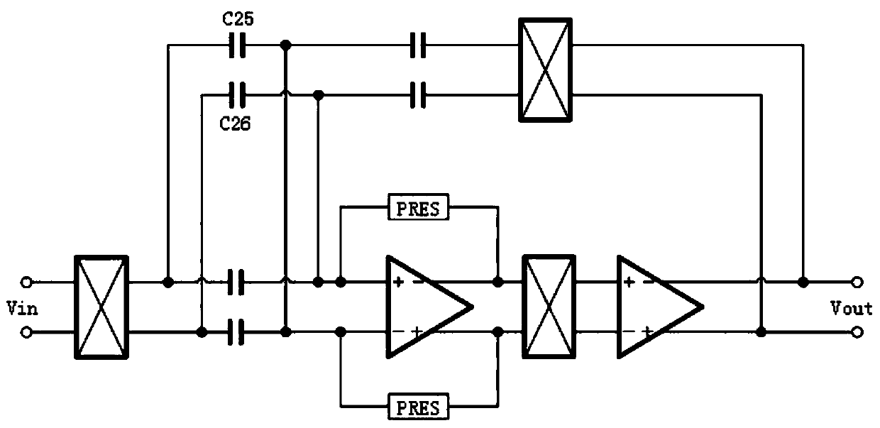
[0056] Such as Image 6 As shown, the first-stage amplifying circuit 33 includes a fourth operational amplifier A4, a fifth operational amplifier A5, a seventh dummy resistor R7, an eighth dummy resistor R8, a ninth dummy resistor R9 and a tenth dummy resistor R10; The non-inverting input terminal of the fourth operational amplifier A4 is sequentially connected in series with the seventh pseudo-resistor R7 and the eighth pseudo-resistor R8, and then connected to the inverting input terminal of the fifth operational amplifier A5, and the seventh pseudo-resistor R7 and the eighth pseudo-resistor A common-mode voltage input terminal is connected between R8, and the output terminal of the fourth operational amplifier A4 passes through the second-stage chopping switch 34, the second-stage amplifying circuit 35 and the negative feedback unit in turn, and then connects the non-phase of the fifth operational amplifier A5. The input terminal is also connected to the inverting input ter...


PUM


Abstract

The invention discloses a chopper amplification circuit adopting a negative impedance compensation technology. The chopper amplification circuit comprises a differential input end, a first-stage chopper switch, a first-stage amplification circuit, a second-stage chopper switch, a second-stage amplification circuit, a negative impedance conversion circuit, a negative feedback unit, an input capacitor and a differential output end, the differential input end is connected with the first-stage chopper switch and is used for accessing a differential voltage signal; an output terminal of the first-stage chopper switch is connected with the first-stage amplifying circuit through an input capacitor; the first-stage amplification circuit is connected with the second-stage chopper switch, the second-stage chopper switch is connected with the second-stage amplification circuit, and the second-stage amplification circuit is connected with the differential output end and is further connected with the feedback input end of the first-stage amplification circuit through the negative feedback unit, and the negative impedance conversion circuit is connected to the signal input end of the first-stageamplification circuit in parallel for reducing the equivalent input capacitance of the first-stage amplification circuit. The circuit has the advantages of high input impedance and high stability, and can be suitable for occasions requiring high input impedance.

Description

technical field [0001] The invention relates to the technical field of analog circuit design, in particular to a chopper amplifier circuit using negative impedance compensation technology. Background technique [0002] Since the chopper amplification technology was proposed in 1948, with the continuous development of integrated circuit technology, it was soon applied to chip integration technology. Chopper amplification technology is a modulation technology that improves the performance of operational amplifiers. Its basic principle is to use an AC modulation signal to modulate low-frequency noise and offset voltage to high-frequency, and then filter to eliminate its influence. It is mainly used for low-frequency weak Low noise amplification of the signal. [0003] A typical full integrated circuit implementation of a chopper amplifier is usually as figure 1 Shown: The differential voltage signal is modulated into a high-frequency AC signal by the chopper switch CH11, and ...

Claims


Application Information

Patent Timeline
Patent Type & Authority Applications(China)
IPC IPC(8): H03F1/56H03F1/34H03F3/45
CPCH03F1/56H03F1/26H03F3/393H03F3/45188H03F3/45645H03F2200/129H03F2200/369H03F2200/271H03F2203/45082H03F2203/45068H03F2203/45074H03F2203/45076H03F2203/45084H03F3/45475H03F3/387
Inventor 梁志明李斌吴朝晖
Owner SOUTH CHINA UNIV OF TECH
Why Eureka
Try Eureka