Check patentability & draft patents in minutes with Patsnap Eureka AI!

Broadband strip line debugging structure with slow wave characteristics and design method thereof

A design method and stripline technology, applied to waveguides, waveguide devices, circuits, etc., can solve the problems of difficult debugging and phase compensation of striplines, and achieve the effect of improving transmission performance and design flexibility

Active Publication Date: 2019-06-28
CHINA ELECTRONIC TECH GRP CORP NO 38 RES INST
View PDF8 Cites 2 Cited by
  • Summary
  • Abstract
  • Description
  • Claims
  • Application Information

AI Technical Summary

Problems solved by technology

[0006] The technical problem to be solved by the present invention lies in the problem that the stripline of the three-dimensional wiring microwave multi-chip module of the prior art stripline transmission system is not easy to debug and difficult to perform phase compensation

Method used


Image

  • Broadband strip line debugging structure with slow wave characteristics and design method thereof
  • Broadband strip line debugging structure with slow wave characteristics and design method thereof
  • Broadband strip line debugging structure with slow wave characteristics and design method thereof

Examples


Embodiment Construction

[0037] The embodiments of the present invention are described in detail below. This embodiment is implemented on the premise of the technical solution of the present invention, and detailed implementation methods and specific operating procedures are provided, but the protection scope of the present invention is not limited to the following implementation example.

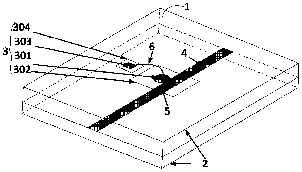
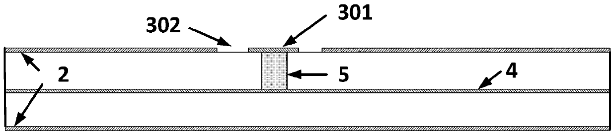
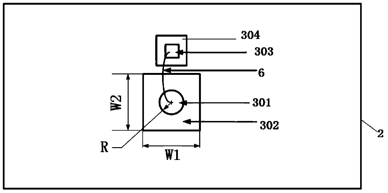
[0038] see figure 1 and combine figure 2 , a broadband stripline debugging structure with slow wave characteristics, applied to a multilayer circuit board, the multilayer circuit board includes several layers of dielectric boards 1, and ground layers 2 and debugging structures 3 are arranged on the several layers of dielectric boards 1 on.

[0039] The several layers of dielectric plates 1 include a surface layer (not marked in the figure), an intermediate layer (not marked in the figure) and a bottom layer (not marked in the figure). The upper dielectric board, the bottom layer is the bottom dielectric board, an...


PUM

PropertyMeasurementUnit
Thicknessaaaaaaaaaa

Abstract

The invention discloses a broadband strip line debugging structure with slow wave characteristics and a design method thereof. The broadband strip line debugging structure is applied to a multi-layercircuit board, the multi-layer circuit board comprises multiple layers of dielectric plates which comprise surface layers, middle layers and bottom layers, the surface layers and the bottom layers ofthe dielectric plates are provided with ground layers, the middle layers of the multiple layers of dielectric plates are provided with stripe lines, the debugging structure and the stripe lines are connected through vertical metal columns filled with metal, and the debugging structure has the slow wave characteristics. According to the invention, the strip line debugging of a microwave multi-chipmodule and the phase compensation are carried out without affecting the transmission performance such as a transmission effect, a return loss, insertion loss and port impedance.

Description

technical field [0001] The invention relates to the technical field of three-dimensional wiring microwave multi-chip module (MMCM) based on a stripline transmission system, and more specifically relates to the detection, debugging and phase adjustment of microwave signals transmitted by an inner stripline in the MMCM. Background technique [0002] With the rapid development of radar and communication technology, the three-dimensional packaging microwave multi-chip component (MMCM) technology based on microwave multilayer circuit board is widely used in miniaturized, lightweight, multi-functional and high-reliability microwave components and systems. By making full use of the inner layer space of microwave multilayer circuit boards, designers can greatly reduce the layout area of ​​the surface layer of the multilayer circuit board and improve the layout flexibility; in addition, compared with the surface layer microstrip line, the inner layer stripline can Achieve low dispers...

Claims


Application Information

Patent Timeline
IPC IPC(8): H01P3/08H01P11/00
Inventor 于鹏飞王光池张孔陈兴国季飞
Owner CHINA ELECTRONIC TECH GRP CORP NO 38 RES INST
Features
  • R&D
  • Intellectual Property
  • Life Sciences
  • Materials
  • Tech Scout
  • Unparalleled Data Quality
  • Higher Quality Content
  • 60% Fewer Hallucinations
Learn More