Semiconductor structure and forming method thereof

A technology of semiconductor and conductive structure, applied in the field of semiconductor structure and its formation, can solve problems such as poor performance of vertical nanowire transistors, and achieve the effect of high integration

Active Publication Date: 2019-07-02
SEMICON MFG INT (SHANGHAI) CORP +1
View PDF4 Cites 0 Cited by
  • Summary
  • Abstract
  • Description
  • Claims
  • Application Information

AI Technical Summary

Problems solved by technology

[0005] However, the performance of ex...

Method used


Image

  • Semiconductor structure and forming method thereof
  • Semiconductor structure and forming method thereof
  • Semiconductor structure and forming method thereof

Examples


Embodiment Construction

[0032] The prior art semiconductor structure has many problems, for example, the performance of the semiconductor structure is poor and the integration level is low.

[0033] Now combine a semiconductor structure to analyze the reasons for the low integration of the existing semiconductor structure:

[0034] Because the conventional planar transistor occupies a large substrate surface, the integration of the semiconductor structure is low. In order to improve the integration of the formed semiconductor structure, a vertical nanowire transistor is proposed.

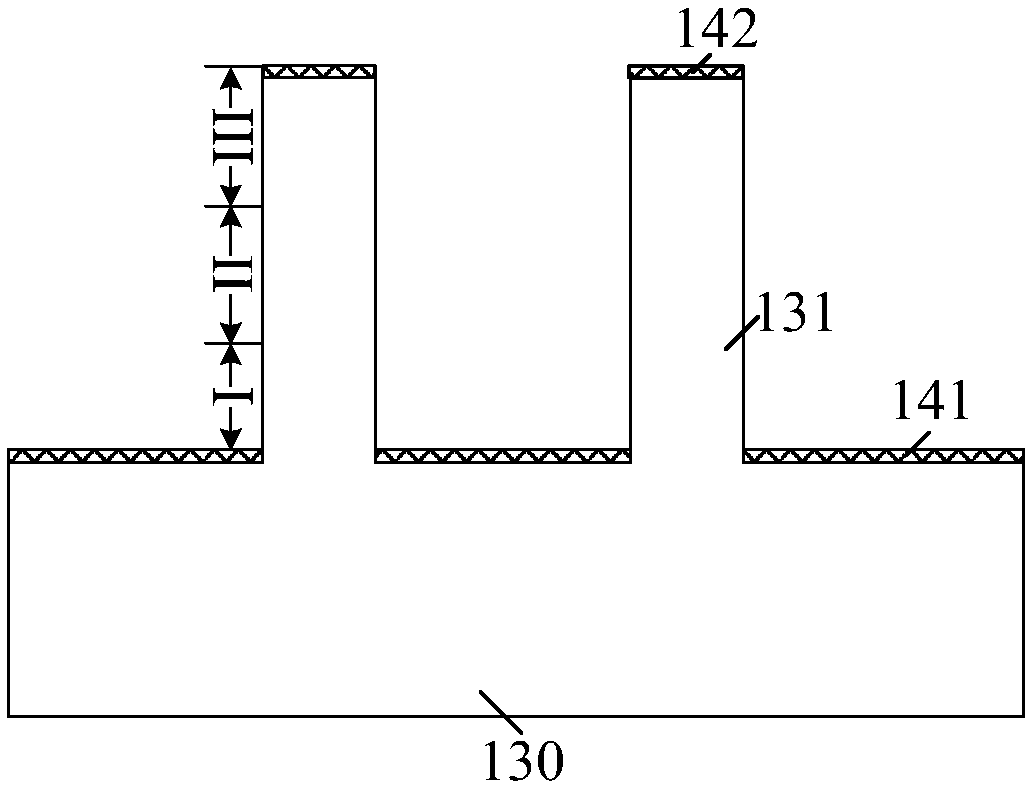
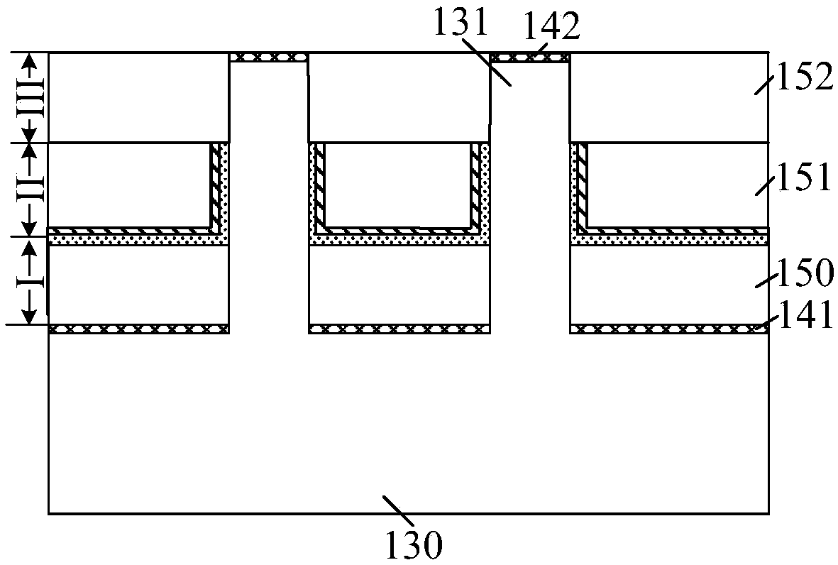
[0035] figure 1 with figure 2 It is a schematic diagram of the structure of each step of a method for forming a vertical nanowire transistor.

[0036] Please refer to figure 1 , A substrate 130 is provided, the surface of the substrate 130 has a fin pillar 131, the fin pillar 131 includes a bottom region I, a channel region II located on the bottom region I, and a top portion located on the channel region II Zone III.

[0037] Co...


PUM

PropertyMeasurementUnit
Thicknessaaaaaaaaaa
Heightaaaaaaaaaa

Abstract

A semiconductor structure and a forming method thereof are provided. The forming method comprises the following steps: forming a spacer covering the side walls of a channel region and a top region ofeach fin column; forming a first conductive structure on the side wall surface of each bottom region with the spacers as masks; removing the spacers after forming the first conductive structures; forming a gate structure on the top of each first conductive structure after removing the spacers, wherein the gate structures are located on the surfaces of the channel regions of the fin columns; and forming a second conductive structure on the top of each gate structure after forming the gate structures, wherein the second conductive structures are located on the surfaces of the top regions of thefin columns. The forming method can improve the integration degree of the formed semiconductor structure.

Description

Technical field [0001] The present invention relates to the technical field of semiconductor manufacturing, in particular to a semiconductor structure and a method of forming the same. Background technique [0002] With the rapid development of semiconductor manufacturing technology, semiconductor devices are moving towards higher component density and higher integration. With the increase in the element density and integration of semiconductor devices, the size of transistors has also become smaller and smaller, and the reduction in the size of transistors has made the short channel effect more and more significant. [0003] In order to reduce the short channel effect, fin-type field effect transistors were born. The gate of the fin-type field effect transistor has a fork-shaped 3D structure similar to a fish fin. The gate of the fin-type field effect transistor can be turned on and off by the multi-side control circuit of the fin, so that the short channel effect of the transis...

Claims


Application Information

Patent Timeline
IPC IPC(8): H01L29/78H01L21/336
CPCH01L29/785H01L21/823431H01L29/66795
Inventor 李勇洪中山
Owner SEMICON MFG INT (SHANGHAI) CORP
Why Eureka
Try Eureka