LED substrate, LED and packaging method of LED

A technology of LED substrates and LED chips, which is applied in the direction of electrical components, circuits, semiconductor devices, etc., can solve the problems of weak resistance to moisture ingress and shortened service life of LED encapsulation adhesives, and achieve enhanced machine placement yield, The effect of improving the binding force and improving the ability to resist moisture ingress

Inactive Publication Date: 2019-07-02
WUHU JUFEI PHOTOELECTRIC TECH CO LTD
View PDF4 Cites 2 Cited by
  • Summary
  • Abstract
  • Description
  • Claims
  • Application Information

AI Technical Summary

Problems solved by technology

However, as the LED packaging and the overall size of the LED continue to decrease, the adhesive surface between the packaging adhesive and the substrate is also getting smaller and smaller, so that the ability of the LED packaging adhesive to resist moisture ingress is also getting weaker and weaker. Shorten the service life of the LED and the soldering yield during later installation

Method used


Image

  • LED substrate, LED and packaging method of LED
  • LED substrate, LED and packaging method of LED
  • LED substrate, LED and packaging method of LED

Examples


Embodiment 1

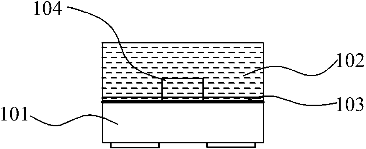
[0031] Aiming at the problem in the prior art that the ability of the LED encapsulant to resist moisture ingress becomes weaker after the solid-type encapsulation is completed due to the reduction in the size of the LED, the present invention provides a solution by prolonging the bond between the encapsulant and the substrate body. Surface area to improve the moisture resistance of the encapsulant. Specifically, the present invention provides a LED substrate, see figure 2 , the LED substrate 1 includes a substrate body 11, and the substrate body 11 includes at least two planes with a difference between them. Preferably, in this embodiment, two planes are set on the substrate body 11 as an example for illustration, and the set The height difference H between the two planes is greater than zero, and it can be understood that the height difference here refers to the vertical distance between the two planes.

[0032] In this embodiment, the substrate body 11 also includes a copp...

Embodiment 2

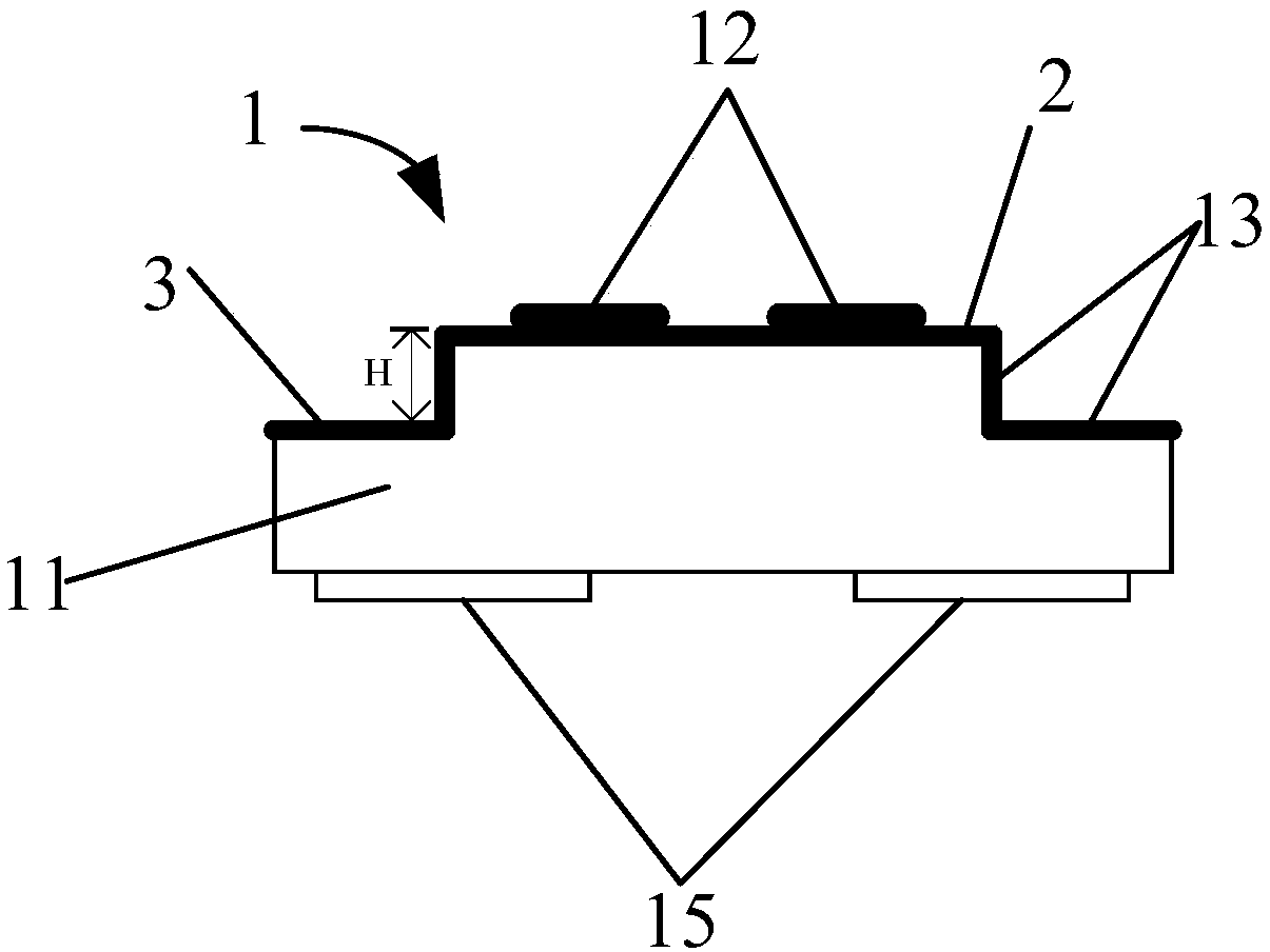
[0044] Please refer to Figure 8 , Figure 8 It is a schematic structural diagram of an LED provided by the present invention. The LED specifically includes an LED chip 21, an encapsulant 22 and an LED substrate 1. Preferably, the LED substrate 1 is the LED substrate provided in the first embodiment above. The LED substrate 1 includes a substrate body 11, and a copper-clad area 12 and a packaging area 13 on the substrate body, wherein the substrate body 11 specifically includes at least two planes with a difference between each other, and the copper-clad area 12 and the packaging area 13 respectively arranged on these two planes; the LED chip 21 is welded on the copper clad area 12 on the LED substrate 1, and the encapsulation glue 22 is pressed onto the encapsulation area 13 by a molding process to be solidified, The LED chip 21 is sealed on the LED substrate 1 .

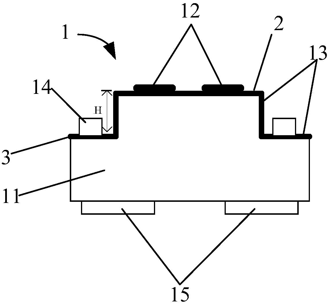
[0045] In this embodiment, at least one geometric step 14 is also provided on the area corresponding to the pa...

Embodiment 3

[0049] See Figure 9 , Figure 9 It is a flow chart of the LED packaging method provided by the present invention. The LED provided in this embodiment includes an LED substrate 1, an LED chip 21 and an encapsulation glue 22, wherein the LED substrate 1 is provided with at least two planes that are not on the same horizontal line , and a copper-clad area and a packaging area are correspondingly provided on these two planes, the copper-clad area is used for soldering the LED chip 21, and the packaging area is used to carry the solid type of packaging glue 22 and fix it on the In order to realize the sealing of the LED chip 21 on the packaging area, in order to adapt to the production and manufacture of the LED, the present invention provides a manufacturing method that can extend the area of ​​the bonding surface between the packaging glue and the LED substrate. Specifically, the packaging The implementation steps of the method include:

[0050] S901, setting at least two plan...


PUM


Abstract

The embodiment of the invention provides an LED substrate, an LED and a packaging method of the LED. The LED substrate comprises a substrate body having at least two planes with height difference, anda copper clad area and a packaging area which are arranged on the substrate body. The copper clad area and the packaging area are correspondingly arranged on the two planes with height difference, and the packaging area is arranged around the copper clad area. Because the copper clad area and the packaging area are correspondingly arranged on the two planes with height difference, the distance between an LED chip and the edge of the substrate body is extended due to the direct height difference between the two planes, the area of the bonding surface between the packaging adhesive and the substrate body is increased, and the moisture resistance of the packaging adhesive and the service life of the LED are improved. The bonding force between the packaging adhesive and the substrate body isenhanced while the area of the bonding surface is further increased, and the yield of later chip surface-mounting on the application side is improved.

Description

technical field [0001] The invention relates to the technical field of LEDs, in particular to an LED substrate, an LED and an LED packaging method. Background technique [0002] In recent years, LED has been playing an important role in the display field of mobile terminals relying on its unique advantages such as low price, low power consumption, high brightness, and long life, and there will be considerable development in a long period of time in the future. space. like figure 1 As shown, most of the current top and chip LEDs are vertically packaged by using a horizontal substrate 101 (ceramic, BT resin, FR4, etc.), and the packaging glue 102 contacts the surface plane 103 of the substrate to seal the LED chip 104 . However, as the LED packaging and the overall size of the LED continue to decrease, the adhesive surface between the packaging adhesive and the substrate is also getting smaller and smaller, so that the ability of the LED packaging adhesive to resist moisture...

Claims


Application Information

Patent Timeline
Patent Type & Authority Applications(China)
IPC IPC(8): H01L33/48H01L33/54H01L33/62
CPCH01L33/486H01L33/54H01L33/62H01L2933/0033H01L2933/005
Inventor 李振宁张志宽邢其彬徐欣荣姚亚澜
Owner WUHU JUFEI PHOTOELECTRIC TECH CO LTD
Why Eureka
Try Eureka