Semiconductor laser module

A laser module, semiconductor technology, applied in the direction of semiconductor lasers, lasers, laser parts, etc., can solve the problems of low power, output spot energy density and quality constraints, and achieve the effect of wide industrial value

Inactive Publication Date: 2019-07-02
FOCUSLIGHT TECH
View PDF16 Cites 2 Cited by
  • Summary
  • Abstract
  • Description
  • Claims
  • Application Information

AI Technical Summary

Problems solved by technology

[0003] As a form of packaging for semiconductor lasers, To packaging can only achieve relatively small power, and the energy density and quality of the output spot are limited. Currently, it can only be used in the field of laser communication, and cannot be used in laser medical and industrial applications. application

Method used


Image

  • Semiconductor laser module
  • Semiconductor laser module
  • Semiconductor laser module

Examples


Embodiment Construction

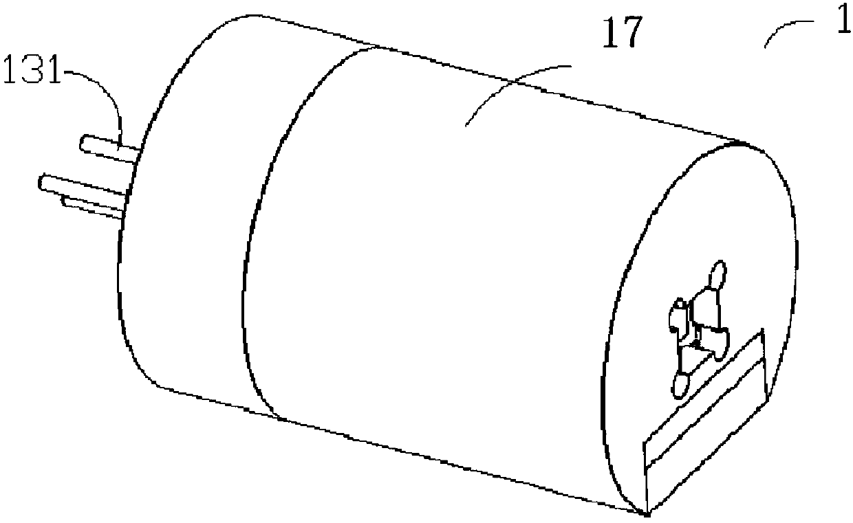
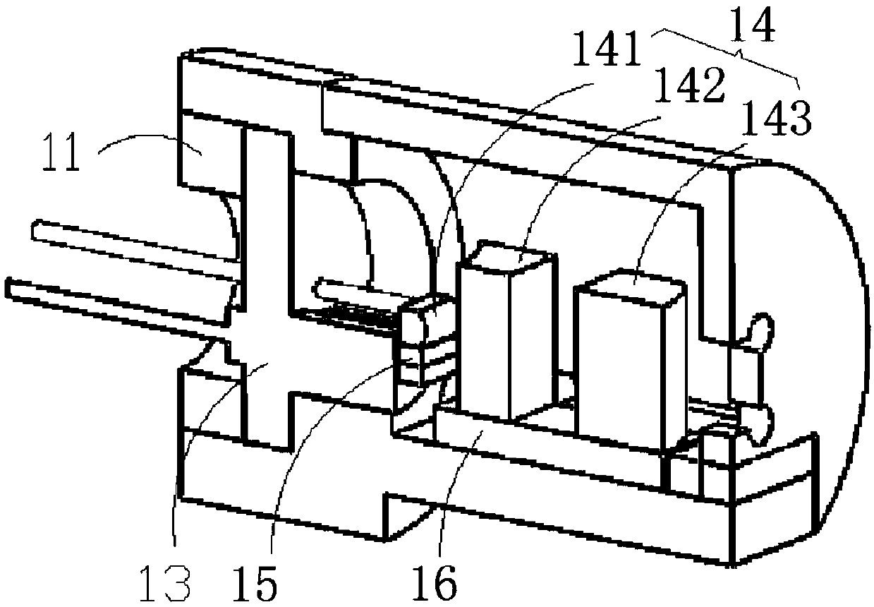
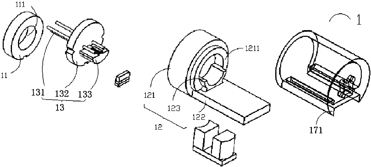
[0040] Hereinafter, various embodiments of the present disclosure will be described more fully with reference to the accompanying drawings. The present disclosure is capable of various embodiments, and adaptations and changes are possible therein. Accordingly, the present disclosure will be described in more detail with reference to specific embodiments illustrated in the accompanying drawings. It is to be understood, however, that there is no intention to limit the various embodiments of the present disclosure to the particular embodiments disclosed herein, but that the present disclosure be construed to cover those falling within the spirit and scope of various embodiments of the present disclosure. All adjustments, equivalents and / or alternatives. In conjunction with the description of the drawings, the same reference numerals designate the same elements.

[0041] Hereinafter, the terms "comprising" or "may include" that may be used in various embodiments of the present d...


PUM


Abstract

The invention provides a semiconductor laser module. The module includes a base, a TO laser and an optical lens group. The base includes an annular connection part and a platform connected to each other. The annular connection part abuts against the TO laser and is used for limiting the TO laser. The optical lens group is placed at the platform. On the basis of the structure, when the semiconductor laser module is implemented, the semiconductor laser module integrates optics, laser and heat dissipation into one body and has the advantages of simple structure, compactness, small volume and highintegration. The modular structure of a semiconductor laser of TO packaging improves the heat dissipation efficiency of the TO packaging and effectively expands the application of the semiconductor laser module in high-power laser medical and industrial scenarios.

Description

technical field [0001] The present invention relates to the technical field of semiconductor laser packaging, in particular, to a semiconductor laser module. Background technique [0002] As an important field of laser application, laser medical treatment develops very rapidly and gradually matures. Semiconductor lasers are especially suitable for the manufacture of medical equipment due to their small size, light weight, long life, low power consumption, and wide wavelength coverage. [0003] As a form of packaging for semiconductor lasers, To packaging can only achieve relatively small power, and the energy density and quality of the output spot are limited. Currently, it can only be used in the field of laser communication, and cannot be used in laser medical and industrial applications. application. Based on this, it is currently a difficult point in this field to research and realize high-power To-packaged semiconductor lasers, improve the heat dissipation efficiency ...

Claims


Application Information

Patent Timeline
Patent Type & Authority Applications(China)
IPC IPC(8): H01S5/024H01S5/022
CPCH01S5/02469H01S5/023H01S5/0233H01S5/0235
Inventor 邢晓绒蔡磊杨凯刘兴胜
Owner FOCUSLIGHT TECH
Why Eureka
Try Eureka