A kind of manufacturing method of semiconductor device and semiconductor device

A manufacturing method and semiconductor technology, applied in the manufacture of semiconductor devices, in the field of semiconductor devices, can solve problems such as high surface peak electric field, increased cost, and poor breakdown stability, achieve high pinch-off voltage, reduce process cost, and high The effect of stability

Active Publication Date: 2021-01-01
CSMC TECH FAB2 CO LTD
View PDF4 Cites 0 Cited by
  • Summary
  • Abstract
  • Description
  • Claims
  • Application Information

AI Technical Summary

Problems solved by technology

For traditional discrete depletion-mode VDMOS devices, in order to improve the pinch-off stability of the device, a threshold voltage (Vt) injection plate is usually added on the basis of the conventional enhanced VDMOS manufacturing process to form a depletion channel on the surface. However, this will increase the cost. At the same time, when the device is working in the on state, due to the high ion concentration near the channel surface, the surface peak electric field is too high, and the breakdown stability becomes poor.

Method used


Image

  • A kind of manufacturing method of semiconductor device and semiconductor device
  • A kind of manufacturing method of semiconductor device and semiconductor device
  • A kind of manufacturing method of semiconductor device and semiconductor device

Examples


Embodiment 1

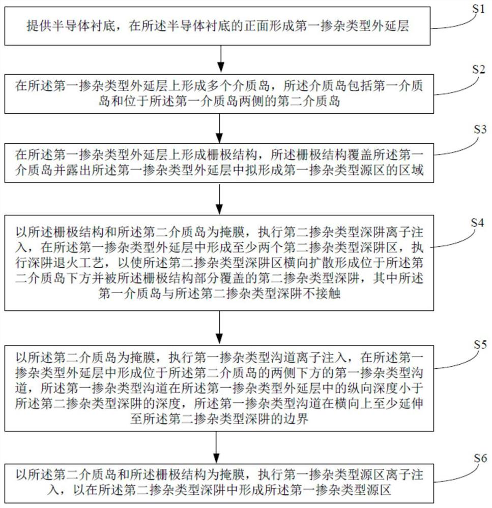
[0040] see below figure 1 and Figures 2A-2G A method for manufacturing a semiconductor device proposed by the present invention is exemplified, wherein, figure 1 It is a flowchart of a method for manufacturing a semiconductor device according to an embodiment of the present invention; Figures 2A-2G based on figure 1A schematic structural diagram of a semiconductor device formed in a method for manufacturing a semiconductor device is shown.

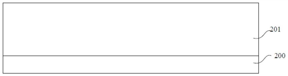
[0041] First, see figure 1 , performing step S1: providing a semiconductor substrate, and forming an epitaxial layer of the first doping type on the front surface of the semiconductor substrate.

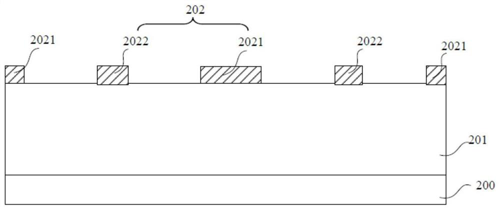
[0042] Such as Figure 2A As shown, a semiconductor substrate 200 is provided, specifically, it may be at least one of the materials mentioned below: Si, Ge, SiGe, SiC, SiGeC, InAs, GaAs, InP, InGaAs or other III / V compound semiconductors , including multilayer structures composed of these semiconductors, or silicon-on-insulator (SOI), si...

Embodiment 2

[0082] The present invention also provides a semiconductor device, which includes the semiconductor device obtained by the manufacturing method in Embodiment 1. The semiconductor device includes:

[0083] semiconductor substrate;

[0084] a first doping type epitaxial layer located on the front side of the semiconductor substrate;

[0085] a dielectric island located on the first doped type epitaxial layer;

[0086] a gate structure located on the first doped type epitaxial layer, the gate structure covering the dielectric island and part of the first doped type epitaxial layer;

[0087] The second doping type deep well is located on both sides of the dielectric island and in the first doping type epitaxial layer, and a part of the second doping type deep well is located below the gate material layer, And the deep well of the second doping type is not in contact with the dielectric island;

[0088] The source region of the first doping type is located on both sides of the ...


PUM

PropertyMeasurementUnit
lengthaaaaaaaaaa
thicknessaaaaaaaaaa
lengthaaaaaaaaaa

Abstract

The present invention provides a manufacturing method of a semiconductor device and a semiconductor device. According to the manufacturing method of the semiconductor device and the semiconductor device, in the formation process of a depletion type device, a medium island is formed as a mask to perform self-alignment ion implantation to form a channel, the depth and the dosage concentration of thechannel region can be accurately controlled by control of the implantation energy and dosage to achieve the pinch-off voltage with high stability so as to omit the step of providing an ion implantation mask by employing the photolithography and the photolithography technique in the ion implantation regulation by the threshold voltage, reduce the process flow and reduce the process cost; and in the process of forming the channel in the depletion type device, the channel ion implantation can be blocked due to the medium island, the concentration of the ions at the lower portion of the medium island is low, so that the breakdown reliability of the semiconductor device in an open state is greatly improved.

Description

technical field [0001] The invention relates to the field of semiconductor manufacturing, in particular to a manufacturing method of a semiconductor device and a semiconductor device. Background technique [0002] Metal-oxide-semiconductor field effect transistors include depletion transistors and enhancement transistors, depletion transistors; when the voltage difference between the gate and source of the depletion transistor is zero, the depletion transistor can be turned on Work, so depletion mode transistors can also be called normally-on transistors. [0003] As the multi-chip packaging technology becomes more and more mature, high-reliability, low-cost discrete depletion-type vertical double-diffused metal-oxide semiconductor field-effect transistor (VDMOS) devices are in line with the mainstream trend of today's power device manufacturing. For traditional discrete depletion-mode VDMOS devices, in order to improve the pinch-off stability of the device, a threshold vol...

Claims


Application Information

Patent Timeline
Patent Type & Authority Patents(China)
IPC IPC(8): H01L21/02H01L21/027
CPCH01L21/02H01L21/0279
Inventor 程诗康顾炎齐从明杨万青张森
Owner CSMC TECH FAB2 CO LTD
Why Eureka
Try Eureka