A method of manufacturing a semiconductor device and an integrated semiconductor device

A manufacturing method and semiconductor technology, applied in the field of semiconductor device manufacturing and integrated semiconductor device, can solve the problems of insignificant leakage effect, increased process cost, increased number of deep wells, etc., so as to improve breakdown reliability and save process steps. , Improve the effect of isolation characteristics

Active Publication Date: 2020-11-03
CSMC TECH FAB2 CO LTD
View PDF6 Cites 0 Cited by
  • Summary
  • Abstract
  • Description
  • Claims
  • Application Information

AI Technical Summary

Problems solved by technology

However, most of the existing different types of VDMOS devices use independent packaging, which will lead to an increase in process costs and disadvantages such as excessive chip area.
[0003] A semiconductor device that integrates an enhanced VDMOS device and a depleted VDMOS device. Since there is usually a potential difference between the source of the depleted device and the source of the enhanced device, it is used in the enhanced device and the depleted device. Set deep wells between them as the isolation structure, however, this method has no obvious effect on reducing leakage, and at the same time, in order to better the isolation effect, it is necessary to increase the number of deep wells, thus wasting a lot of chip area

Method used


Image

  • A method of manufacturing a semiconductor device and an integrated semiconductor device
  • A method of manufacturing a semiconductor device and an integrated semiconductor device
  • A method of manufacturing a semiconductor device and an integrated semiconductor device

Examples


Embodiment 1

[0039] In order to solve the technical problems in the prior art, the invention provides a manufacturing method of a semiconductor device and an integrated semiconductor device.

[0040] In the following, the manufacturing process of the semiconductor device and the semiconductor device of the present invention will be illustrated by taking the manufacturing process of the VDMOS semiconductor device as an example. It should be understood that the description of this embodiment using the manufacturing process of the VDMOS semiconductor device as an example is only exemplary Any manufacturing method of a semiconductor device integrating a depletion-mode device and an enhancement-mode device is applicable to the present invention.

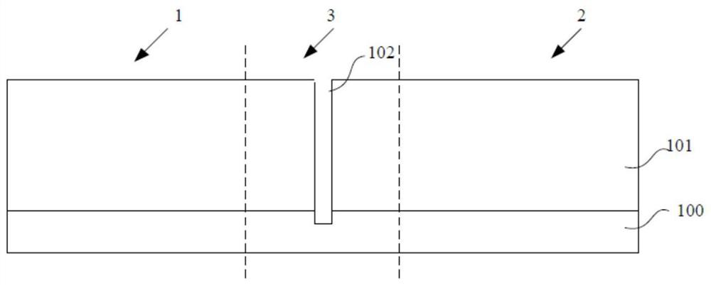
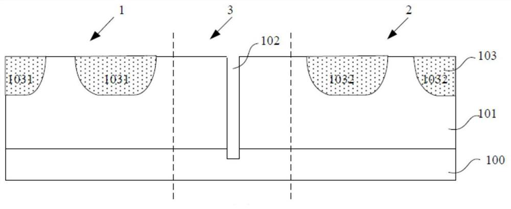
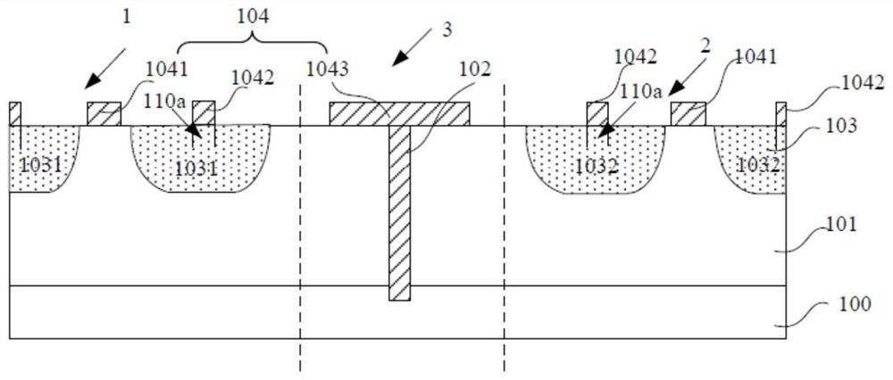
[0041] see below Figures 1A-1G , figure 2 A method for manufacturing a semiconductor device proposed by the present invention is exemplified, Figures 1A-1GIt is a schematic structural diagram of a semiconductor device formed in a method for manufac...

Embodiment 2

[0100] The present invention also provides an integrated semiconductor device, which includes the integrated semiconductor device prepared according to the method described in the first embodiment.

[0101] see below Figure 1G , to exemplarily describe the structure of the semiconductor device of the present invention. The integrated semiconductor device includes: a semiconductor substrate 100, specifically, the semiconductor substrate 100 may be at least one of the materials mentioned below: Si, Ge, SiGe, SiC, SiGeC, InAs, GaAs, InP, InGaAs or other III / V compound semiconductors, including multilayer structures composed of these semiconductors, or silicon-on-insulator (SOI), silicon-on-insulator (SSOI), silicon-germanium-on-insulator (S-SiGeOI), insulator Silicon germanium-on-insulator (SiGeOI) and germanium-on-insulator (GeOI), etc. Exemplarily, the semiconductor substrate in this embodiment is of the first doping type.

[0102] It should be noted that, in this specifica...


PUM

PropertyMeasurementUnit
lengthaaaaaaaaaa
thicknessaaaaaaaaaa

Abstract

The invention provides a manufacturing method of a semiconductor device and an integrated semiconductor device. During the manufacturing process of the semiconductor device integrated with an enhancement device and a depletion device, a dielectric island on an epitaxial layer and a trench in the epitaxial layer are formed. In the process of forming the channel of the depletion device, because the existence of the dielectric island blocks the implantation of channel ions, the ion concentration under the dielectric island is low, which greatly improves the breakdown reliability of the device in the on state; at the same time, due to The existence of the dielectric island increases the thickness of the gate dielectric layer, reduces the gate capacitance, and reduces the switching loss of the device. Setting trenches in the epitaxial layer as the isolation structure of the enhancement-mode device and the depletion-mode device improves the isolation characteristics between the enhancement-mode device and the depletion-mode device on the one hand, and reduces the chip area occupied by the isolation structure on the other hand.

Description

technical field [0001] The invention relates to the field of semiconductor manufacturing, in particular to a method for manufacturing a semiconductor device and an integrated semiconductor device. Background technique [0002] Vertical double-diffused metal oxide field effect devices (VDMOS) include enhancement mode and depletion mode, which have the advantages of good on-off characteristics and low power consumption, and are widely used in LED drivers and power adapters. However, most of the existing VDMOS devices of different types adopt independent packaging, which will bring disadvantages such as increase of process cost and excessive chip area. [0003] A semiconductor device that integrates an enhanced VDMOS device and a depletion-type VDMOS device. Since there is usually a potential difference between the source of the depletion-type device and the source of the enhancement-type device, it is used in the enhancement-type device and the depletion-type device. Set deep...

Claims


Application Information

Patent Timeline
Patent Type & Authority Patents(China)
IPC IPC(8): H01L29/78H01L29/739H01L29/06H01L27/088H01L27/082H01L21/8236H01L21/8222
CPCH01L29/7802H01L29/0649H01L29/7393H01L27/0883H01L27/082H01L21/8236H01L21/8222H01L27/088H01L21/823481H01L29/7828H01L29/66734H01L29/66666H01L29/42368H01L29/7803H01L29/42376H01L29/7395H01L29/66333H01L29/66712H01L27/0617H01L29/0653H01L21/76283H01L21/76224H01L21/266H01L21/823878
Inventor 程诗康顾炎张森
Owner CSMC TECH FAB2 CO LTD
Why Eureka
Try Eureka