A method of manufacturing a semiconductor device and an integrated semiconductor device

A manufacturing method and semiconductor technology, which is applied in the manufacture of semiconductor devices and the field of integrated semiconductor devices, can solve problems such as increased process costs, increased device power consumption, and insufficient depletion, so as to improve breakdown reliability and reduce gate Capacitance, process cost reduction effect

Active Publication Date: 2020-10-13
CSMC TECH FAB2 CO LTD
View PDF4 Cites 0 Cited by
  • Summary
  • Abstract
  • Description
  • Claims
  • Application Information

AI Technical Summary

Problems solved by technology

However, most of these existing semiconductor devices are independently packaged, which brings disadvantages such as increased process costs and excessive chip area.
[0003] A method of integrating an enhanced VDMOS device and a depleted VDMOS device semiconductor device is based on the conventional enhanced VDMOS manufacturing process. It is often necessary to add a Vt injection plate to form a depleted channel on the surface, and the process is complicated. cost increase
However, when the depletion-mode VDMOS device works in the on-state, due to the high concentration near the channel surface, the depletion will be insufficient, resulting in an excessively high surface peak electric field and poor breakdown stability; at the same time, there are usually Severe working environments such as surge currents can easily lead to thermal burnout of the device during the process of passing the avalanche current; in the case of high frequency, the power consumption of the device will increase significantly

Method used


Image

  • A method of manufacturing a semiconductor device and an integrated semiconductor device
  • A method of manufacturing a semiconductor device and an integrated semiconductor device
  • A method of manufacturing a semiconductor device and an integrated semiconductor device

Examples


Embodiment 1

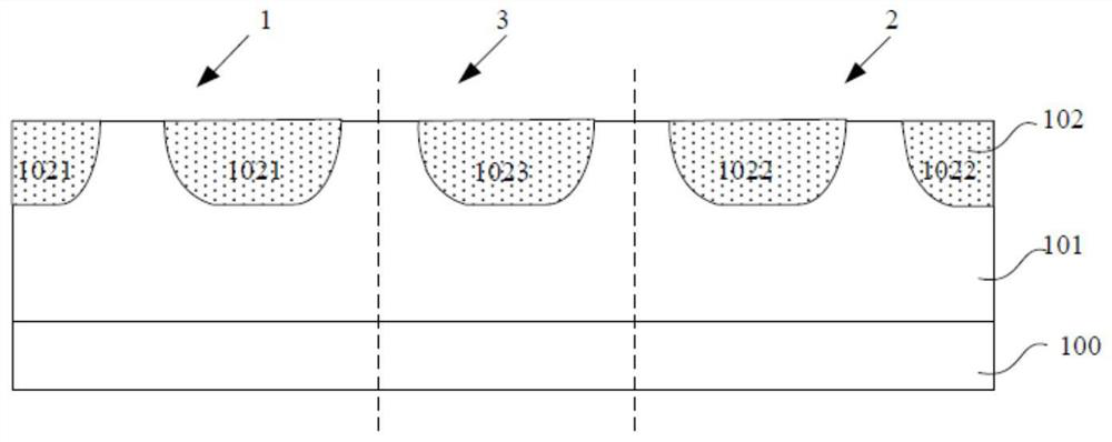
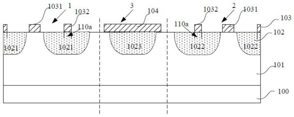
[0037] see below Figures 1A-1G , figure 2 A method for manufacturing a semiconductor device and a semiconductor device proposed in the present invention are exemplarily described. in, Figures 1A-1G is a schematic structural view of a semiconductor device formed in a method for manufacturing a semiconductor device according to an embodiment of the present invention, figure 2 It is a flowchart of a manufacturing method of a semiconductor device according to an embodiment of the present invention.

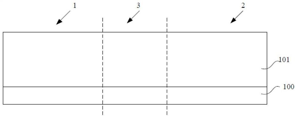
[0038] First, see figure 2 , performing step S1: providing a semiconductor substrate of the first doping type, and forming an epitaxial layer of the first doping type having a first region and a second region on the front surface of the semiconductor substrate of the first doping type.

[0039] Such as Figure 1AAs shown, the semiconductor substrate 100 of the first doping type is provided, specifically, it may be at least one of the materials mentioned below: Si, Ge, SiGe, ...

Embodiment 2

[0088] The present invention also provides an integrated semiconductor device, which includes the semiconductor device prepared according to the method in the first embodiment.

[0089] see below Figure 1G , to exemplarily describe the structure of the integrated semiconductor device of the present invention. The integrated semiconductor device includes: a semiconductor substrate 100 of a first doping type. The semiconductor substrate 100 of the first doping type, specifically, may be at least one of the materials mentioned below: Si, Ge, SiGe, SiC, SiGeC, InAs, GaAs, InP, InGaAs or other III / V Compound semiconductors, including multilayer structures composed of these semiconductors, or silicon-on-insulator (SOI), silicon-on-insulator (SSOI), silicon-germanium-on-insulator (S-SiGeOI), silicon-germanium-on-insulator (SiGeOI) ) and germanium on insulator (GeOI), etc.

[0090] It should be noted that, in this specification, the first doping type and the second doping type gen...


PUM

PropertyMeasurementUnit
lengthaaaaaaaaaa
thicknessaaaaaaaaaa

Abstract

The invention provides a manufacturing method of a semiconductor device and an integrated semiconductor device. In the method, a dielectric island is formed on an epitaxial layer during the manufacturing process of the semiconductor device. The implantation of channel ions is ensured, and the ion concentration under the dielectric island is low, which greatly improves the breakdown reliability of the device in the on state; at the same time, due to the existence of the dielectric island, the thickness of the gate dielectric layer increases, reducing the gate Capacitors reduce switching losses of the device. At the same time, using the dielectric island as a mask during the manufacturing process, the source region of the first doping type can be formed by self-alignment, which saves a photolithography plate and reduces the process cost.

Description

technical field [0001] The invention relates to the field of semiconductor manufacturing, in particular to a method for manufacturing a semiconductor device and an integrated semiconductor device. Background technique [0002] Existing semiconductor devices include enhancement mode and depletion mode semiconductor devices, such as vertical double diffused metal oxide field effect devices (VDMOS) including enhancement mode VDMOS devices and depletion mode VDMOS devices, which have good on-off characteristics and low power consumption. Advantages, widely used in LED drivers, power adapters, etc. However, most of these existing semiconductor devices are individually packaged, which brings disadvantages such as increased process cost and excessive chip area. [0003] A method of integrating an enhanced VDMOS device and a depleted VDMOS device semiconductor device is based on the conventional enhanced VDMOS manufacturing process. It is often necessary to add a Vt injection plate...

Claims


Application Information

Patent Timeline
Patent Type & Authority Patents(China)
IPC IPC(8): H01L29/78H01L21/336
CPCH01L29/7802H01L29/66712H01L29/7828H01L29/42376H01L29/1095H01L21/761H01L21/8236H01L27/088H01L21/8222H01L27/082H01L27/0883H01L29/0649H01L29/7393H01L21/26513H01L21/266H01L29/086H01L29/42364
Inventor 程诗康顾炎张森
Owner CSMC TECH FAB2 CO LTD
Why Eureka
Try Eureka