An integrated semiconductor device and electronic device

A technology for semiconductors and devices, applied in the field of integrated semiconductor devices and electronic devices, can solve the problems of increased process cost, insufficient depletion, thermal burnout of devices, etc., to improve breakdown reliability, save chip area, and reduce switching loss. Effect

Active Publication Date: 2021-07-09
CSMC TECH FAB2 CO LTD
View PDF0 Cites 0 Cited by
  • Summary
  • Abstract
  • Description
  • Claims
  • Application Information

AI Technical Summary

Problems solved by technology

However, most of these existing products are independently packaged, which brings disadvantages such as increased process costs and excessive chip area.
[0003] In an integrated semiconductor device integrating an enhanced VDMOS device and a depletion-type VDMOS device, when the depletion-type VDMOS device is in the on-state operation, due to the high concentration near the channel surface, the depletion will be insufficient, causing the surface peak electric field to exceed High, the breakdown stability becomes poor; at the same time, there are usually harsh working environments such as surge currents in the actual load circuit, and it is easy to cause thermal burnout of the device during the process of passing the avalanche current; in the case of high frequency , the power consumption of the device will increase significantly

Method used


Image

  • An integrated semiconductor device and electronic device
  • An integrated semiconductor device and electronic device

Examples


Embodiment 1

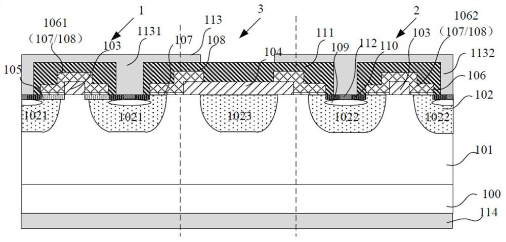
[0033] In the following, the integrated semiconductor device of the present invention will be illustrated by taking an integrated VDMOS semiconductor device as an example. It should be understood that the description of this embodiment by taking an example of an integrated VDMOS semiconductor device is only exemplary, and any integrated depletion-mode device and The manufacturing method of the integrated semiconductor device of the enhanced device is applicable to the present invention.

[0034] In order to solve the problems in the prior art, the present invention provides an integrated semiconductor device. face to face figure 1 The structure of the semiconductor device of the present invention is described exemplarily.

[0035] Integrated semiconductor device described in the present invention comprises:

[0036] semiconductor substrate;

[0037] a first doping type epitaxial layer, located on the front side of the semiconductor substrate, including a first region, a sec...

Embodiment 2

[0072] In this embodiment, an integrated IGBT device is also provided, and the integrated IGBT device includes a depletion-type IGBT device and an enhancement-type IGBT device. Specifically, the semiconductor substrate in Embodiment 1 is set to the second doping type, that is, the semiconductor substrate is a P-type substrate, while the formation positions and doping types of other components in Embodiment 1 remain unchanged. Specifically , the IGBT device includes:

[0073] a semiconductor substrate of a second doping type;

[0074] a first doping type epitaxial layer, located on the front side of the semiconductor substrate, including a first region, a second region and a third region, and an isolation structure is provided in the third region;

[0075] A second doping type deep well located in the first doping type epitaxial layer, including at least two located in the first region and at least two located in the second region;

[0076] a dielectric island, located on the...

Embodiment 3

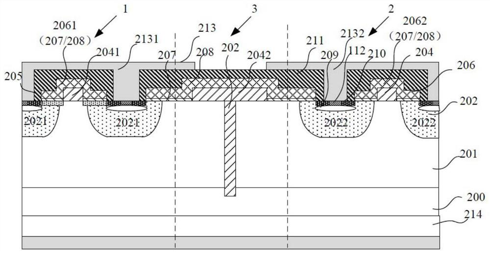
[0084] Refer below figure 2 The structure of another integrated semiconductor device according to the present invention will be described.

[0085] like figure 2 As shown, an integrated semiconductor device according to the present invention includes a semiconductor substrate 200 . The semiconductor substrate 200, specifically, may be at least one of the materials mentioned below: Si, Ge, SiGe, SiC, SiGeC, InAs, GaAs, InP, InGaAs or other III / V compound semiconductors, including these Multi-layer structure of semiconductor, or silicon on insulator (SOI), silicon on insulator (SSOI), silicon germanium on insulator (S-SiGeOI), silicon germanium on insulator (SiGeOI) and germanium on insulator ( GeOI) and so on. Exemplarily, the semiconductor substrate is of the first doping type.

[0086] It should be noted that, in this specification, the first doping type and the second doping type generally refer to P type or N type, wherein the first doping type is opposite to the seco...


PUM

PropertyMeasurementUnit
lengthaaaaaaaaaa
thicknessaaaaaaaaaa

Abstract

The invention provides an integrated semiconductor device and an electronic device, which can integrate a depletion device and an enhancement device on one semiconductor device, and package the two devices at the same time, saving process flow and chip area. At the same time, the gate structure Dielectric islands are arranged below. During the process of channel formation of depletion-type devices, the existence of dielectric islands blocks the implantation of channel ions, and the ion concentration below the dielectric islands is low, which greatly improves the breakdown reliability of devices in the on state. At the same time, due to the existence of the dielectric island, the thickness of the gate dielectric layer is increased, the gate capacitance is reduced, and the switching loss of the device is reduced.

Description

technical field [0001] The invention relates to the field of semiconductor manufacturing, in particular to an integrated semiconductor device and an electronic device. Background technique [0002] Existing semiconductor devices include enhancement mode and depletion mode semiconductor devices, such as vertical double diffused metal oxide field effect devices (VDMOS) including enhancement mode VDMOS devices and depletion mode VDMOS devices, which have good on-off characteristics and low power consumption. Advantages, widely used in LED drivers, power adapters, etc. However, most of these existing products are independently packaged, which brings disadvantages such as increased process cost and excessive chip area. [0003] In an integrated semiconductor device integrating an enhanced VDMOS device and a depletion-type VDMOS device, when the depletion-type VDMOS device is in the on-state operation, due to the high concentration near the channel surface, the depletion will be ...

Claims


Application Information

Patent Timeline
Patent Type & Authority Patents(China)
IPC IPC(8): H01L27/088H01L29/78H01L27/082H01L29/739
CPCH01L27/0883H01L29/7802H01L27/082H01L29/7395H01L29/739H01L21/823481H01L21/8236H01L21/823487H01L29/7828H01L29/1095H01L29/42376H01L21/76224
Inventor 程诗康顾炎张森
Owner CSMC TECH FAB2 CO LTD
Why Eureka
Try Eureka