
Method for removing protruding block defects on polysilicon surface by slow grinding and semiconductor process method

A polysilicon and semiconductor technology, applied in semiconductor/solid-state device manufacturing, grinding equipment, grinding machine tools, etc., can solve the problems of excessive removal, fast removal rate, and affecting the performance of device structures, etc., achieve high cleaning effect, reduce loss, Easy to clean effect

Active Publication Date: 2019-07-09
CHANGXIN MEMORY TECH INC
View PDF7 Cites 0 Cited by
  • Summary
  • Abstract
  • Description
  • Claims
  • Application Information

AI Technical Summary

Problems solved by technology

[0004] In view of the above-mentioned shortcoming of prior art, the object of the present invention is to provide a kind of slow grinding method that removes bump defect on polysilicon surface, is used to solve the problem of using existing alkaline grinding that contains silicon dioxide abrasive particles in the prior art When the buffer solution removes bump defects on the surface of the polysilicon layer, the removal rate is too fast, and it is easy to remove too much polysilicon layer while removing the bump defects, thereby affecting the performance of the final device structure.

Method used


Image

  • Method for removing protruding block defects on polysilicon surface by slow grinding and semiconductor process method
  • Method for removing protruding block defects on polysilicon surface by slow grinding and semiconductor process method
  • Method for removing protruding block defects on polysilicon surface by slow grinding and semiconductor process method

Examples


Embodiment 1

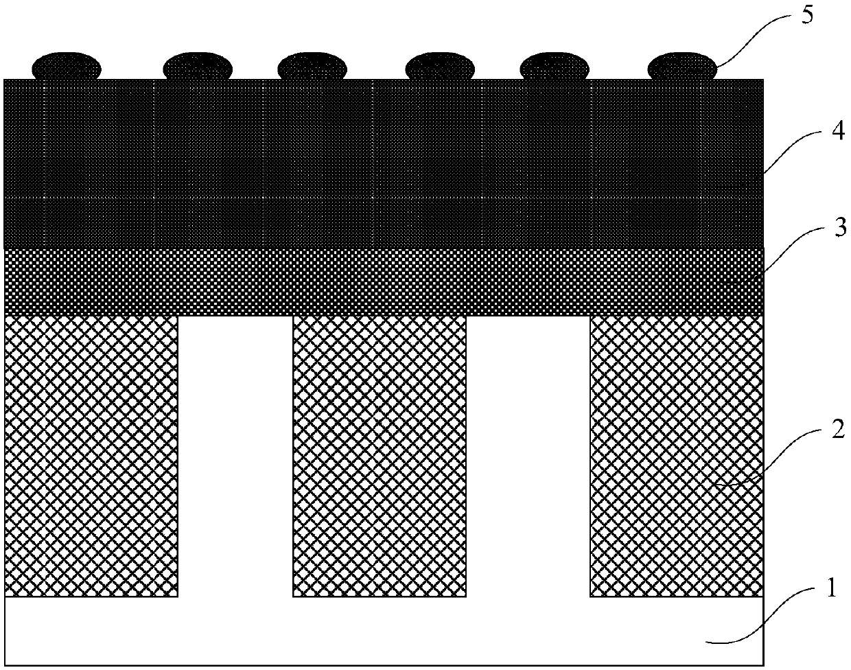
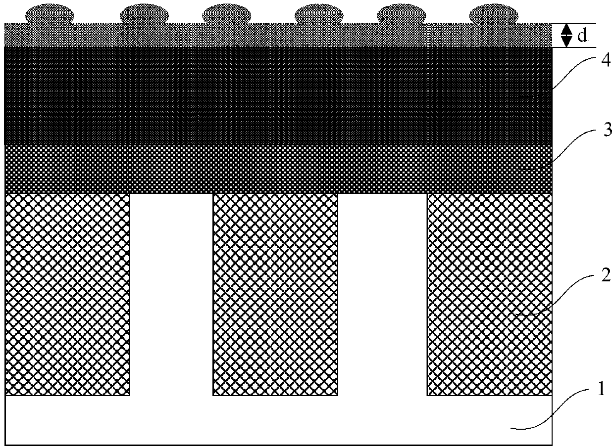
[0046] Such as Figure 1 to Figure 3 shown. The present invention provides a method for removing bump defects on the surface of polysilicon by slow grinding. The method for removing bump defects on the surface of polysilicon by slow grinding at least includes the following steps:

[0047] 1) placing a semiconductor structure comprising a polysilicon layer having bump defects formed on a surface of the polysilicon layer in a chemical mechanical polishing apparatus; and,

[0048] 2) Carrying out chemical mechanical grinding on the polysilicon layer with a grinding buffer containing cerium oxide abrasive particles to remove bump defects on the surface of the polysilicon layer, wherein the grinding buffer is weakly acidic to prevent the The polysilicon of the polysilicon layer is oxidized to form silicon dioxide during chemical mechanical polishing.

[0049] In step 1), see figure 2 Step S1 in and figure 2 , placing the semiconductor structure including the polysilicon layer...

Embodiment 2

[0069] see Figure 4 , the present invention also provides a semiconductor process method, the semiconductor process method comprising the following steps:

[0070] Step S10: preparing a semiconductor structure comprising a polysilicon layer having bump defects formed on the surface of the polysilicon layer; and,

[0071] Step S20: Treat the surface of the polysilicon layer of the semiconductor structure by using the slow grinding method described in the first embodiment to remove bump defects on the polysilicon surface.

[0072] In step S10, see Figure 4 , preparing a semiconductor structure comprising a polysilicon layer, the surface of the polysilicon layer is formed with bump defects.

[0073] As an example, the semiconductor structure may be any existing structure containing the polysilicon layer, specifically, the semiconductor structure may be any existing semiconductor structure in which a polysilicon layer has just been formed, the The underlying polysilicon layer...


PUM


Abstract

The invention provides a method for removing protruding block defects on a polysilicon surface by slow grinding and a semiconductor processing method. The method for removing the protruding block defects on the polysilicon surface by slow grinding comprises the following steps that (1) a semiconductor structure including a polysilicon layer is disposed in a chemical mechanical planarization device, and the protruding block defects are formed on the surface of the polysilicon layer; and (2) chemical mechanical planarization is performed on the polysilicon layer by using a grinding buffer solution containing cerium oxide abrasive particles to remove the protruding block defects on the surface of the polysilicon layer, and the grinding buffer solution is weakly acidic to prevent polysilicon in the polysilicon layer from being oxidized to form silica in the chemical mechanical planarization process. The polysilicon layer is subjected to chemical mechanical planarization by using the acidicgrinding buffer solution containing the cerium oxide abrasive particles, since the removal rate of polysilicon by the cerium oxide abrasive particles is low in an acidic environment, the thickness ofthe removed polysilicon layer can be effectively controlled while removing the protruding block defects on the surface of the polysilicon layer, and thus the loss of the polysilicon layer is reduced.

Description

technical field [0001] The invention relates to the technical field of semiconductor technology, in particular to a method for removing bump defects on the surface of polysilicon by slow grinding and a semiconductor technology method. Background technique [0002] In the existing semiconductor technology, the application of polysilicon is more and more extensive. In the existing polysilicon formation process, after the polysilicon layer is formed, due to the limitations of the polysilicon growth process and the presence of impurities in the polysilicon growth environment, bump defects will be formed on the upper surface of the formed polysilicon layer, and the bump defects The existence of the polysilicon layer will affect the quality of the subsequent process and the performance of the finally formed device structure, and needs to be removed after forming the polysilicon layer. [0003] In order to make the surface of the polysilicon layer have higher flatness after removi...

Claims


Application Information

Patent Timeline
Patent Type & Authority Applications(China)
IPC IPC(8): B24B37/10B24B37/04B24B37/005B24B49/16H01L21/321
CPCB24B37/005B24B37/0056B24B37/044B24B37/10B24B49/16H01L21/3212
Inventor 蔡长益
Owner CHANGXIN MEMORY TECH INC
Learn More