Manufacturing method of thin film touch sensor and thin film touch sensor

A technology of touch sensing and manufacturing methods, which is applied in the input/output process of instruments, data processing, calculation, etc., and can solve the problems of stacking offset of each layer, small stacking offset of lines, and low efficiency of exposure alignment , to achieve the effects of small line stack offset, precise exposure alignment, stable and controllable shape and size changes

Active Publication Date: 2022-06-21
LENS TECH CHANGSHA
View PDF6 Cites 0 Cited by
  • Summary
  • Abstract
  • Description
  • Claims
  • Application Information

AI Technical Summary

Problems solved by technology

[0005] The first object of the present invention is to provide a method for manufacturing a thin-film touch sensor, which can effectively solve the problems of low exposure alignment efficiency and stacking offset of each layer of circuits, accurate exposure alignment, high efficiency, and circuit stacking Small offset, high product yield, in addition, thin film touch sensors can also be produced in sheets

Method used


Image

  • Manufacturing method of thin film touch sensor and thin film touch sensor
  • Manufacturing method of thin film touch sensor and thin film touch sensor
  • Manufacturing method of thin film touch sensor and thin film touch sensor

Examples


Embodiment 1

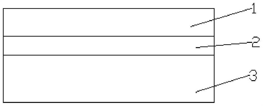
[0068] A manufacturing method of a thin film touch sensor, comprising the following steps:

[0069] (a) Bake the rigid carrier covered with the film substrate, the baking temperature is 130°C, and the baking time is 60min; wherein the film substrate is a PET film substrate, the rigid carrier is a glass plate, and the film substrate The adhesive between the material and the rigid carrier is acrylic adhesive;

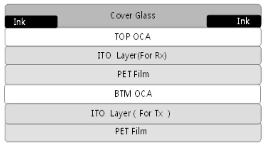
[0070] (b) Making multi-layer touch circuits:

[0071] The first ITO coating;

[0072] The first ITO line process: photoresist coating, soft baking, exposure, development, hard baking, etching and stripping photoresist, the soft baking temperature is 110 ℃, after baking, let it stand for 3 minutes, and the exposure table temperature is controlled at 25 ℃;

[0073] The first OC line process: OC photoresist coating, soft baking, exposure, development and solid baking, the soft baking temperature is 110 ° C, the soft baking time is 3 minutes, after baking, let stand for 3 ...

Embodiment 2

[0081] A manufacturing method of a thin-film touch sensor is different from Embodiment 1 in that the baking temperature is 140° C., the baking time is 40 minutes, and other steps and parameters are the same as those in Embodiment 1.

Embodiment 3

[0083] A manufacturing method of a thin-film touch sensor is different from Embodiment 1 in that the baking temperature is 120° C., the baking time is 60 minutes, and other steps and parameters are the same as those in Embodiment 1.


PUM

PropertyMeasurementUnit
thicknessaaaaaaaaaa
elastic modulusaaaaaaaaaa

Abstract

The invention relates to the field of touch screens, and specifically provides a method for manufacturing a thin-film touch sensor and the thin-film touch sensor. The manufacturing method of the thin film touch sensor comprises the following steps: (a) baking the rigid carrier plate covered with the film substrate, the baking temperature is 120-150°C, and the baking time is 30-60min; b) Make a multi-layer touch circuit, wherein, the rest time after soft baking is 2-10min, and the temperature of the exposure table is 25-35°C; (c) combine the film substrate of the multi-layer touch circuit with the rigid The board is separated to obtain the thin film touch sensor. This method can effectively solve the problems of circuit stack offset and low exposure alignment efficiency of each layer when making a touch sensing layer on a film. The exposure alignment is accurate, the efficiency is high, and the line stack offset is small, and the product is good. In addition, it can also produce thin film touch sensors in sheet form.

Description

technical field [0001] The present invention relates to the field of touch screens, and in particular, to a method for manufacturing a thin-film touch sensor and a thin-film touch sensor. Background technique [0002] Touch screen has been widely used in mobile phones, tablets, e-books and other products due to the new human-computer interaction method. At present, according to the material of the touch screen, it is generally divided into glass touch screen and thin film touch screen. Thin-film touch screens are further divided into GFF, GF2, GF and other structures. Compared with glass touch screens, thin-film touch screens have the advantages of lightness, thinness and low cost, and have become the most important touch solutions. [0003] GF2 is a touch sensing structure that integrates Tx and Rx circuits on a single-layer film. This single-layer film structure can achieve a thickness of less than 50 μm, which is especially suitable for 3D glass curved surface lamination,...

Claims


Application Information

Patent Timeline
Patent Type & Authority Patents(China)
IPC IPC(8): G06F3/041
CPCG06F3/0412G06F2203/04103
Inventor 周群飞项小鑫贾成兰
Owner LENS TECH CHANGSHA
Why Eureka
Try Eureka