Device and method of detecting polished quartz wafer shallow scratch

A technology for quartz wafers and polishing wafers, which is used in measurement devices, optical testing of flaws/defects, and material analysis by optical means to improve efficiency and stability and reduce workstations.

Pending Publication Date: 2019-07-12
RES INST OF ZHEJIANG UNIV TAIZHOU
View PDF3 Cites 5 Cited by
  • Summary
  • Abstract
  • Description
  • Claims
  • Application Information

AI Technical Summary

Problems solved by technology

[0005] The technical problem to be solved by the present invention is to provide a device and method for detecting shallow scratches on polished quartz wafers, which can replace manual sorting of polished wafer defects and improve efficiency and stability

Method used


Image

  • Device and method of detecting polished quartz wafer shallow scratch
  • Device and method of detecting polished quartz wafer shallow scratch
  • Device and method of detecting polished quartz wafer shallow scratch

Examples


Embodiment Construction

[0044]The following will clearly and completely describe the technical solutions in the embodiments of the present invention with reference to the accompanying drawings in the embodiments of the present invention. Obviously, the described embodiments are some of the embodiments of the present invention, but not all of them. Based on the embodiments of the present invention, all other embodiments obtained by persons of ordinary skill in the art without making creative efforts belong to the protection scope of the present invention.

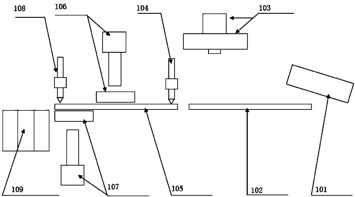
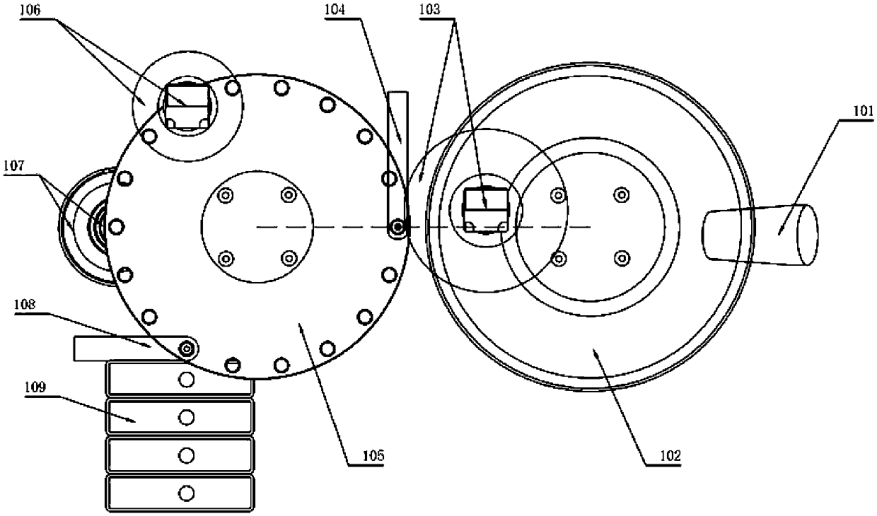
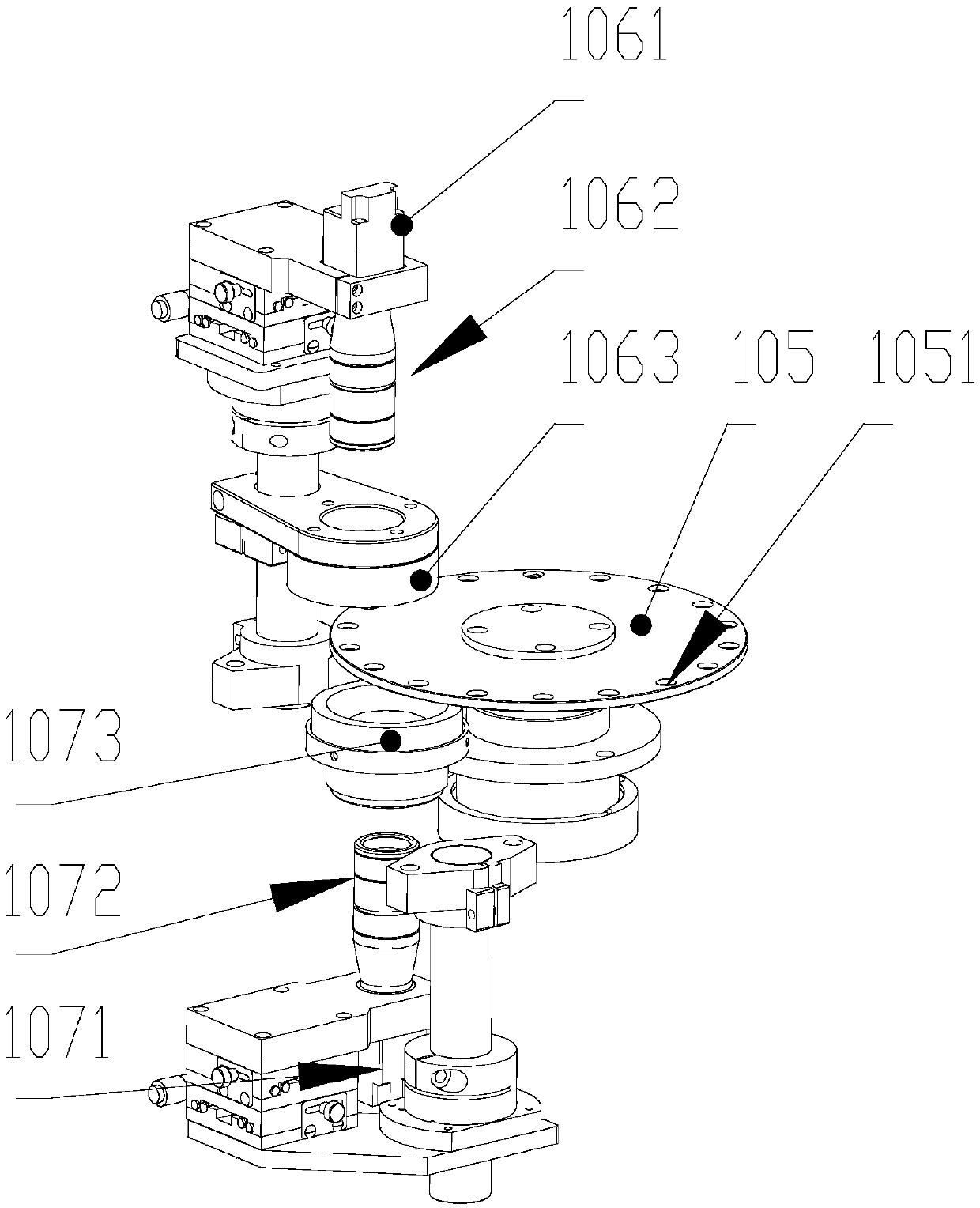
[0045] see figure 1 Shown is a schematic diagram of the structure of the device for detecting shallow scratches on polished quartz wafers according to an embodiment of the present invention, see figure 2 Shown is the top view of the device structure of the polished quartz wafer shallow scratch detection of the embodiment of the present invention, see image 3 Shown is a schematic diagram of a part of the detection mechanism of the embodiment of t...


PUM

PropertyMeasurementUnit
thicknessaaaaaaaaaa
thicknessaaaaaaaaaa

Abstract

The invention discloses a device and a method of detecting a polished quartz wafer shallow scratch. The device comprises a material feed cylinder, a wafer taking tray, a positioning module, a wafer taking sucking head, a detection tray, a front detection module, a back detection module, a wafer placing sucking head and a wafer accommodation box, wherein the material feed cylinder is used for scattering polished wafers onto the wafer taking tray based on certain vibration frequency under control of a main procedure, the wafer taking tray is designed to turn by a small angle clockwise and anticlockwise precisely, so as to distribute the polished wafers onto the wafer taking tray uniformly disorderly to be taken up one by one layer, the positioning module comprises a positioning camera, a lens and a light source, is above the wafer taking tray, and is used for positioning and imaging the polished wafer on the wafer taking tray, so as to calculate coordinates of the polished wafer, whereinthe coordinates comprise a step size and a turning angle.

Description

technical field [0001] The invention belongs to the technical field of quartz wafer detection, and in particular relates to a device and method for detecting shallow scratches on a polished quartz wafer. Background technique [0002] Quartz wafer is the core device of crystal oscillator. Quartz crystal oscillator (crystal oscillator) provides time reference for electronic equipment and plays an extremely important role in the electronic information industry. Quartz wafer product specifications The diagonal size is within 1-8mm. It is a rectangular crystal. After the surface is ground and extremely polished, the thickness is thin (less than 50um), the friction coefficient is small, and it is extremely smooth; the grinding and polishing process produces missing corners and bright spots. , Chipping, deep scratches and shallow scratches and other defects, the appearance of the product will affect the resonance frequency. [0003] At present, for the inspection of polished quart...

Claims


Application Information

Patent Timeline
Patent Type & Authority Applications(China)
IPC IPC(8): G01N21/95G01N21/01
CPCG01N21/9501G01N21/9503G01N21/01G01N2021/0112
Inventor 余建安陈浙泊林晨宽陈镇元吴荻苇
Owner RES INST OF ZHEJIANG UNIV TAIZHOU
Why Eureka
Try Eureka