Check patentability & draft patents in minutes with Patsnap Eureka AI!

Power semiconductor devices having gate trenches with implanted sidewalls and related methods

A gate trench, semiconductor technology, applied in the direction of semiconductor devices, semiconductor/solid-state device manufacturing, transistors, etc., can solve problems such as complex manufacturing processing

Pending Publication Date: 2019-07-19
CREE INC
View PDF9 Cites 11 Cited by
  • Summary
  • Abstract
  • Description
  • Claims
  • Application Information

AI Technical Summary

Problems solved by technology

Gate Trench MOSFETs can provide enhanced performance but typically require more complex manufacturing processes

Method used


Image

  • Power semiconductor devices having gate trenches with implanted sidewalls and related methods
  • Power semiconductor devices having gate trenches with implanted sidewalls and related methods
  • Power semiconductor devices having gate trenches with implanted sidewalls and related methods

Examples


Embodiment Construction

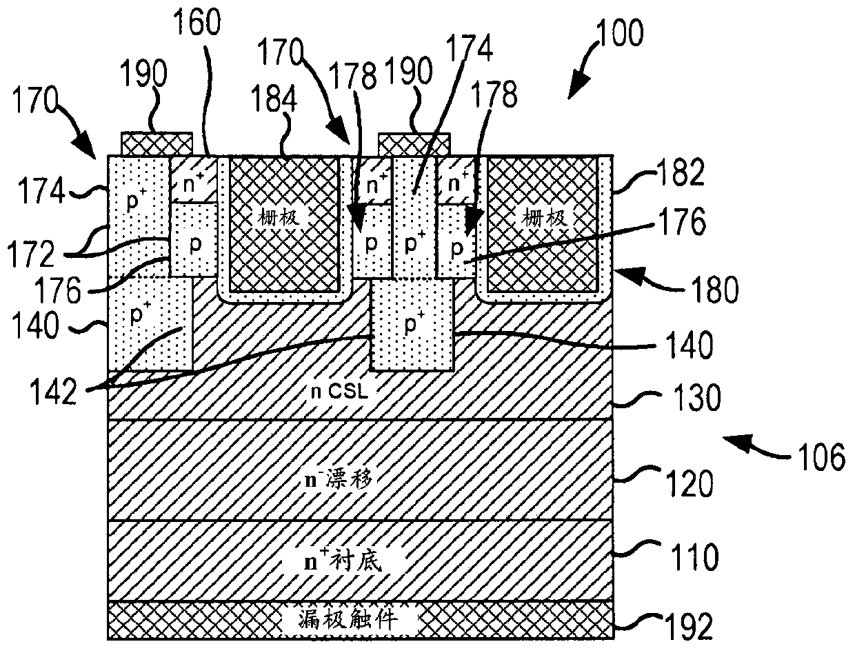
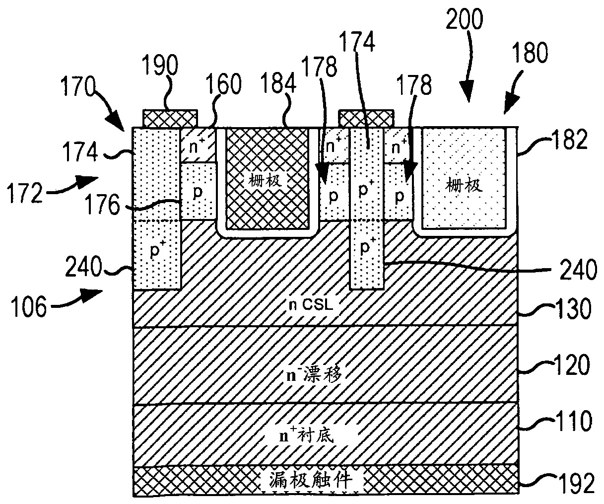
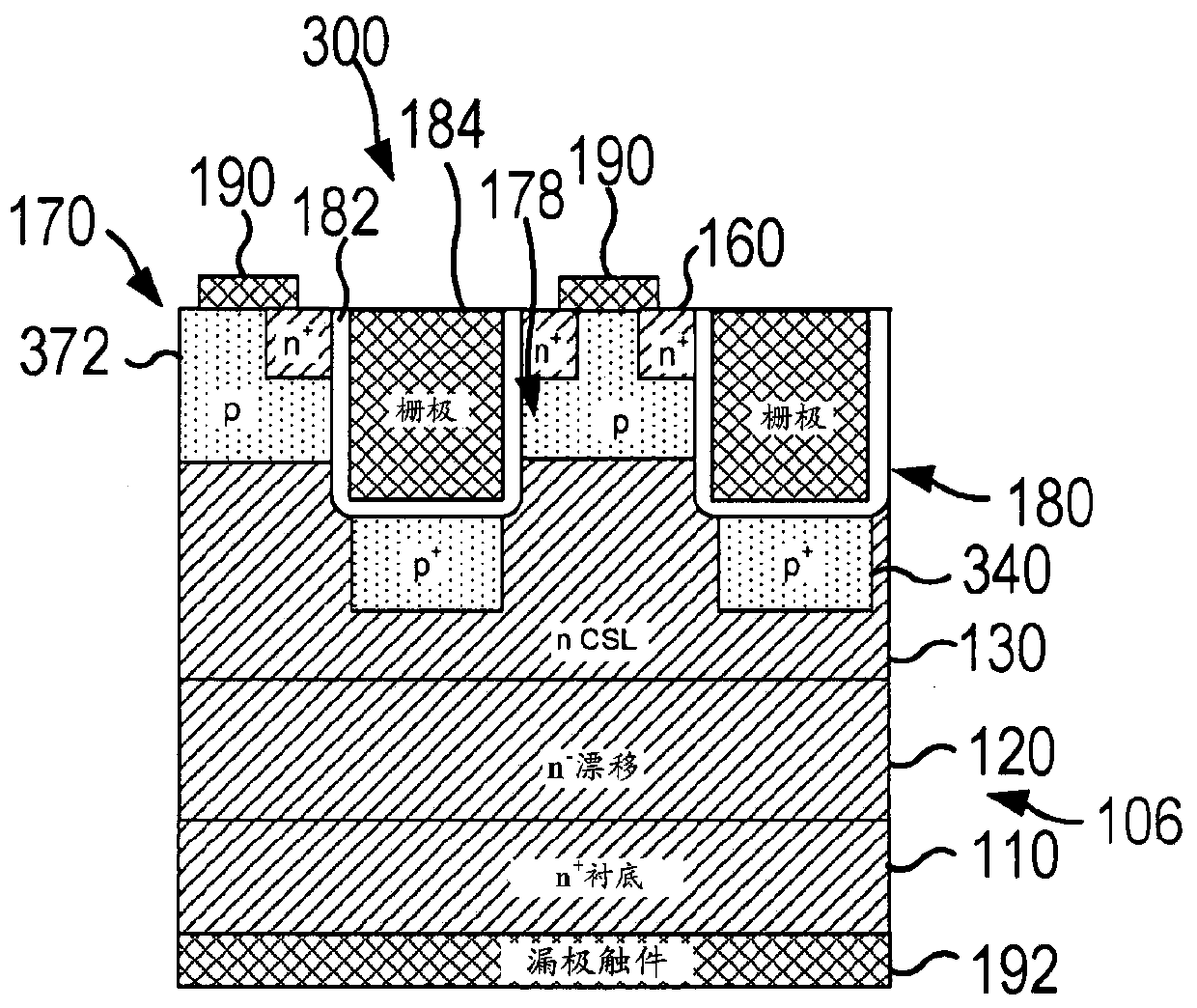
[0064] One challenge in fabricating wide bandgap semiconductor power devices is that it can be more difficult to dope wide bandgap semiconductor materials with impurities to impart n-type or p-type conductivity in certain regions of the power semiconductor device. This is especially true in vertical power devices that include gate trenches, since it is often desirable to form regions of the first conductivity type within layers of the second conductivity type at deep levels within the device, such as from the upper surface of the device From 1-5 microns or more. This can create challenges when fabricating power semiconductor devices in silicon carbide or other wide bandgap semiconductor materials.

[0065] The main methods of doping a semiconductor material with n-type and / or p-type dopants are (1) doping the semiconductor material during its growth, (2) diffusing the dopant into the semiconductor material and (3) using ion implantation To selectively inject dopants into a se...


PUM


Abstract

Semiconductor devices include a semiconductor layer structure having a wide band-gap semiconductor drift region having a first conductivity type. A gate trench is provided in an upper portion of the semiconductor layer structure, the gate trench having first and second opposed sidewalls that extend in a first direction in the upper portion of the semiconductor layer structure. These devices further include a deep shielding pattern having a second conductivity type that is opposite the first conductivity type in the semiconductor layer structure underneath a bottom surface of the gate trench, and a deep shielding connection pattern that has the second conductivity type in the first sidewall of the gate trench. The devices include a semiconductor channel region that has the first conductivity type in the second sidewall of the gate trench.

Description

[0001] US Government Statement of Interest [0002] This invention was made with Government support under Cooperative Agreement No. W911NF-12-2-0064 awarded by the Army Research Laboratory. The government has certain rights in this invention. technical field [0003] The present invention relates to power semiconductor devices, and more particularly, to power semiconductor devices having gate trenches and methods of making such devices. Background technique [0004] Power semiconductor devices are used to carry high currents and support high voltages. A variety of power semiconductor devices are known in the art, including, for example, power metal oxide semiconductor field effect transistors (“MOSFETs”), bipolar junction transistors (“BJTs”), insulated gate bipolar transistors (“IGBTs”), junction Barrier Schottky diodes, gate turn-off transistors ("GTOs"), MOS controlled thyristors, and various other devices. These power semiconductor devices are typically fabricated fro...

Claims


Application Information

Patent Timeline
IPC IPC(8): H01L21/336H01L29/78H01L29/06H01L29/10H01L29/739
CPCH01L29/66068H01L29/66348H01L29/7397H01L29/1095H01L29/1608H01L29/2003H01L29/0619H01L29/0692H01L29/0623H01L29/66734H01L29/7813H01L29/7811H01L29/4236H01L27/088
Inventor D·J·里切特恩沃尔纳E·R·万布鲁特B·胡尔A·V·苏沃洛弗C·卡派尔
Owner CREE INC
Features
  • R&D
  • Intellectual Property
  • Life Sciences
  • Materials
  • Tech Scout
  • Unparalleled Data Quality
  • Higher Quality Content
  • 60% Fewer Hallucinations
Learn More