Through-silicon contact structure and method of forming the same

A contact and contact opening technology, applied in the field of through-silicon contact structure and its formation

Active Publication Date: 2020-03-27
YANGTZE MEMORY TECH CO LTD
View PDF4 Cites 0 Cited by
  • Summary
  • Abstract
  • Description
  • Claims
  • Application Information

AI Technical Summary

Problems solved by technology

As the critical dimensions of semiconductor devices in integrated circuits shrink to achieve higher device densities and faster operating speeds, the RC delay introduced by the associated TSC structure will become a major problem

Method used


Image

  • Through-silicon contact structure and method of forming the same
  • Through-silicon contact structure and method of forming the same
  • Through-silicon contact structure and method of forming the same

Examples


Embodiment Construction

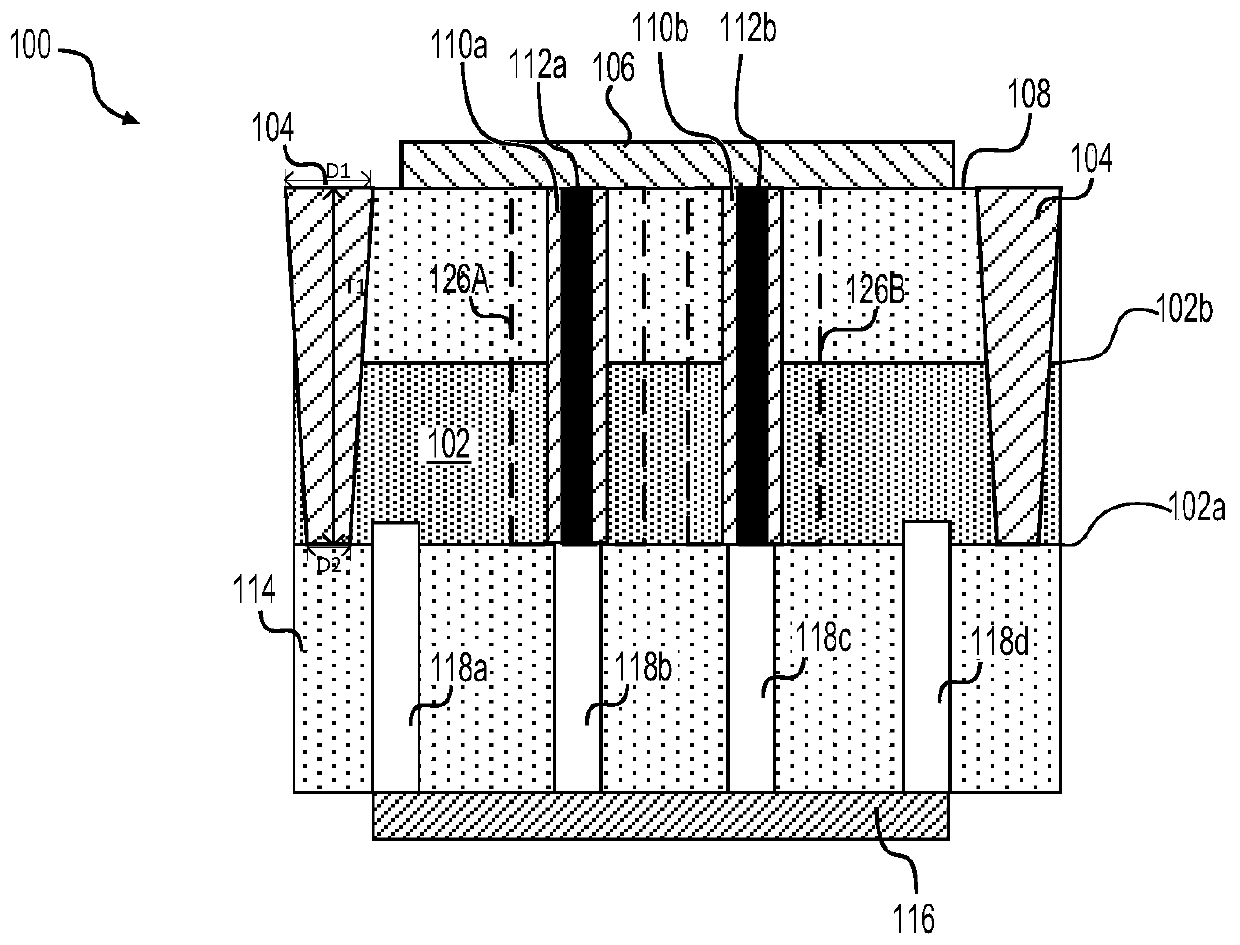
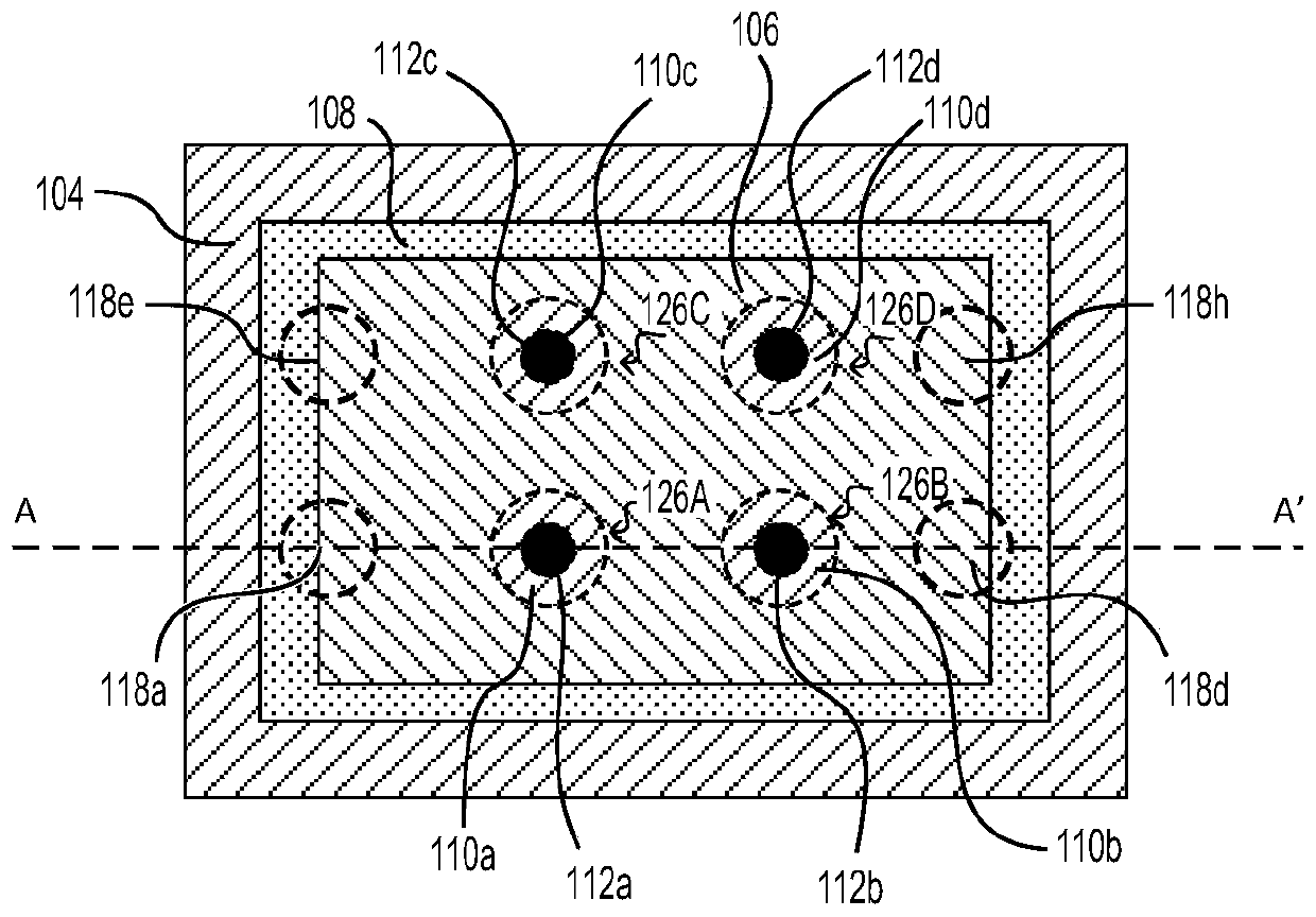
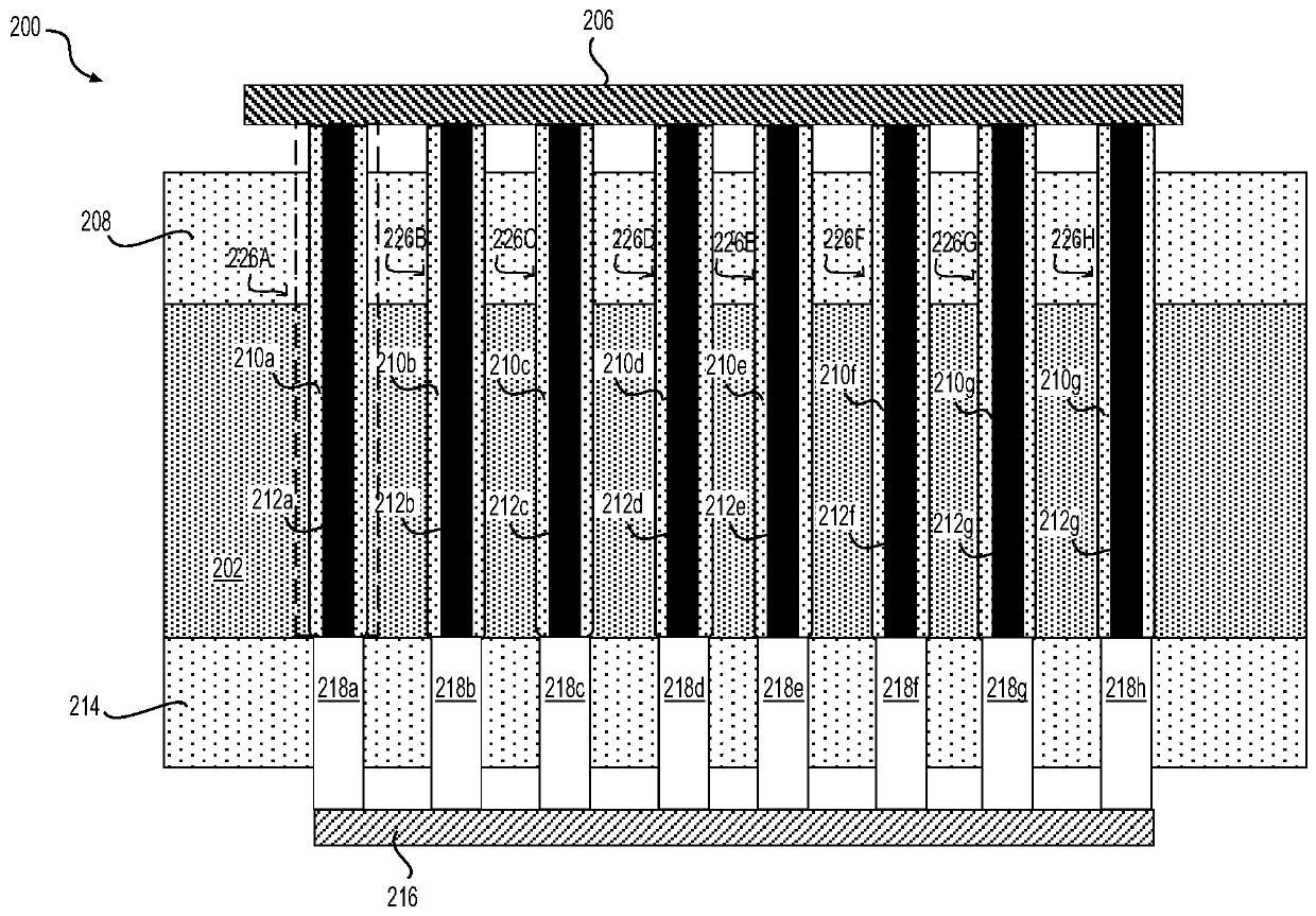
[0023] The following disclosure provides many different embodiments, or examples, for implementing different features of the presented subject matter. Specific examples of components and arrangements are described below to simplify the present disclosure. Of course, these are examples only and are not meant to be limiting. For example, forming a first feature on or over a second feature appearing in the description below may include embodiments in which the first and second features are features that are formed in direct contact, and may also include embodiments in which the first feature and the second feature are formed in direct contact. An embodiment in which an additional feature is formed between the first feature and the second feature so that the first feature and the second feature may not be in direct contact. Also, the present disclosure may repeat numbers and / or letters in various examples. This repetition is for purposes of simplicity and clarity and does not in...


PUM


Abstract

In a TSC structure, a first dielectric layer is formed over a first major surface of a substrate. The substrate includes an opposing second major surface. A TSC is formed in the first dielectric layer and the substrate such that the TSC extends through the first dielectric layer and into the substrate. A conductive plate electrically coupled to the TSC is formed over the first dielectric layer. An isolation trench is formed in the substrate to surround and be spaced from the conductive plate. A second dielectric layer is formed on the second major surface of the substrate. A first plurality of vias extending into the substrate and connected to the TSC are formed in the second dielectric layer. A second plurality of vias extending into the substrate, but not connected to the TSC, are formed in the second dielectric layer.

Description

Background technique [0001] Through silicon contacts (TSCs) are widely used in the semiconductor industry. A TSC is a vertical electrical connection that runs completely through the silicon wafer or die. TSC technology is important in creating 3D packages and 3D integrated circuits. TSCs provide interconnection of vertically aligned electronic devices by significantly reducing the complexity and overall size of internal wiring of multi-chip electronic circuits. TSC technology offers higher interconnect and device densities and shorter connection lengths than conventional packaging technologies. [0002] An associated TSC structure includes a TSC opening through a substrate, a barrier layer formed along sidewalls of the TSC opening, and a conductive material filled in the TSC opening. As the critical dimensions of semiconductor devices in integrated circuits shrink to achieve higher device densities and faster operating speeds, the RC delay introduced by the associated TSC s...

Claims


Application Information

Patent Timeline
Patent Type & Authority Patents(China)
IPC IPC(8): H01L23/48H01L21/768H01L21/762
CPCH01L23/481H01L21/76898H01L21/76224H01L23/485H01L2224/05647H01L2224/05624H01L2224/0361H01L2224/0362H01L2224/03452H01L2224/0345H01L24/05H01L24/03H01L2224/0557H01L2224/05553H01L2924/1434H01L2924/14H01L2924/00014H01L21/76831H01L23/535
Inventor 陈亮刘威S-F·S·鞠
Owner YANGTZE MEMORY TECH CO LTD
Why Eureka
Try Eureka