Antenna packaging structure with air chamber and packaging method

An encapsulation method and encapsulation structure technology, which can be applied to antenna supports/installation devices, antennas, antenna parts, etc., can solve the problems of large loss of antenna encapsulation structure, and achieve the advantages of reducing package size, improving stability and reducing loss. Effect

Pending Publication Date: 2019-07-23
SJ SEMICON JIANGYIN CORP
View PDF0 Cites 2 Cited by
  • Summary
  • Abstract
  • Description
  • Claims
  • Application Information

AI Technical Summary

Problems solved by technology

[0005] In view of the above-mentioned shortcomings of the prior art, the purpose of the present invention is to provide an antenna packaging structure and packaging method with an air chamber, which is used to solve the problem of large loss in the antenna packaging structure in the prior art

Method used


Image

  • Antenna packaging structure with air chamber and packaging method
  • Antenna packaging structure with air chamber and packaging method
  • Antenna packaging structure with air chamber and packaging method

Examples


Embodiment 1

[0051] like Figure 1 to Figure 14 As shown, the present embodiment provides an antenna packaging method with an air cavity, and the packaging method includes the following steps:

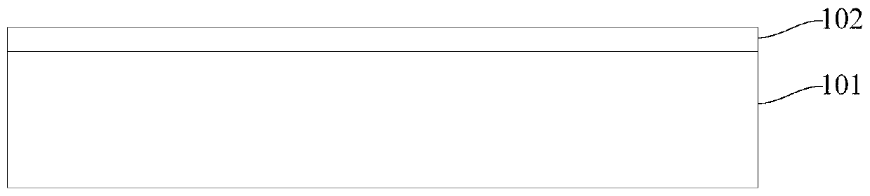
[0052] like figure 1 As shown, step 1) is firstly performed to provide a support base 101 on which the separation layer 102 is formed.

[0053] As an example, the supporting base 101 includes one of a glass substrate, a metal substrate, a semiconductor substrate, a polymer substrate and a ceramic substrate. In this embodiment, the support base 101 is selected as a glass substrate, the cost of the glass substrate is low, the separation layer 102 is easy to be formed on the surface of the glass substrate, and the difficulty of the subsequent peeling process can be reduced.

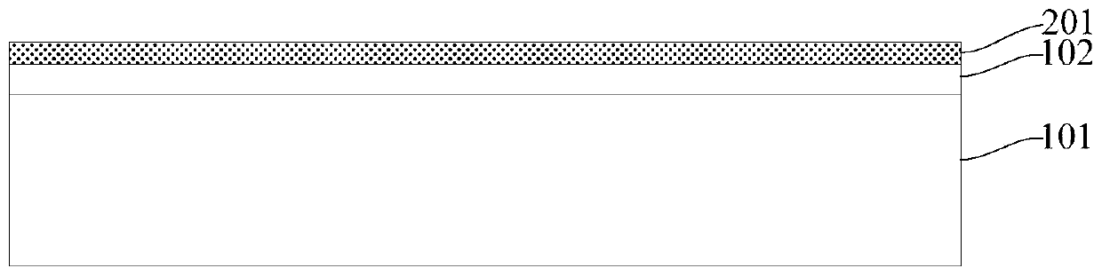
[0054] As an example, the separation layer 102 includes a light-to-heat conversion layer (LTHC), which is formed on the support substrate 101 by a spin-coating process, and then cured and shaped by a curing process. The perfor...

Embodiment 2

[0086] like Figure 15 As shown, this embodiment provides an antenna packaging structure and packaging method with an air cavity, and its basic steps and structure are as in Embodiment 1, wherein the difference from Embodiment 1 lies in that the first part of the substrate 601 Both sides are bonded to the chamber side wall 205 so that the antenna metal layer 603 is located outside the air chamber. The packaging structure and method can make the antenna metal layer 603 exposed on the top of the antenna packaging structure, which can facilitate the electrical connection between it and other components, and can enhance the efficiency of sending and receiving signals of the antenna metal layer 603 .

[0087] As mentioned above, the antenna packaging structure and packaging method with an air cavity of the present invention have the following beneficial effects:

[0088] The present invention can integrate all active components or passive components in one packaging structure thro...


PUM


Abstract

The invention provides an antenna packaging structure with an air chamber and a packaging method. the structure comprises a rewiring layer, a chamber side wall, a substrate, an antenna circuit chip and a metal bump. The rewiring layer comprises a first surface and a second surface which are opposite to each other, the chamber side wall is formed on the second surface of the rewiring layer, the substrate comprises a first surface and a second surface which are opposite to each other, the antenna metal layer is formed on the first surface of the substrate, the substrate is bonded to the chamberside wall, and the substrate, the chamber side wall and the rewiring layer define an air chamber, the antenna circuit chip is electrically connected to the first surface of the rewiring layer, and themetal bump is formed on the first surface of the rewiring layer so as to realize electrical lead-out of the rewiring layer. The air chamber is arranged below the antenna metal layer, and compared with other packaging materials, the loss of antenna signals can be greatly reduced, so that the transmitting and receiving efficiency of the antenna is effectively enhanced.

Description

technical field [0001] The invention belongs to the field of semiconductor packaging, and in particular relates to an antenna packaging structure and a packaging method with an air cavity. Background technique [0002] Due to the progress of science and technology, various high-tech electronic products have been developed to facilitate people's life, including various electronic devices, such as notebook computers, mobile phones, tablet computers (PADs), and the like. [0003] With the popularization of these high-tech electronic products and the increase of people's demand, in addition to the substantial increase of various functions and applications configured in these high-tech products, especially in order to meet people's mobile needs, the function of wireless communication has been added. Therefore, people can use these high-tech electronic products at any place or at any time through these high-tech electronic devices with wireless communication functions. Thereby gr...

Claims


Application Information

Patent Timeline
Patent Type & Authority Applications(China)
IPC IPC(8): H01L23/66H01L23/485H01L23/488H01L21/60H01Q1/22
CPCH01L23/482H01L23/66H01L24/03H01L2224/0231H01L2224/02331H01L2224/02333H01L2224/02381H01Q1/2283
Inventor 陈彦亨林正忠吴政达
Owner SJ SEMICON JIANGYIN CORP
Why Eureka
Try Eureka