Reading structure of mask memory

A memory and mask technology, applied in the field of readout structure of memory, can solve the problems of not setting control signals, influence of process tolerance, waste of chip area, etc., and achieve the effects of low power consumption, reduced power consumption, and safe reading

Active Publication Date: 2019-07-26
JIANGSU HAIDONG SEMICON TECH CO LTD
View PDF9 Cites 0 Cited by
  • Summary
  • Abstract
  • Description
  • Claims
  • Application Information

AI Technical Summary

Problems solved by technology

In this structure, the generation of the reference voltage has a large correlation with the working voltage, that is, different power supply voltages will lead to different reference voltages; in addition, in order to ensure symmetry, a real ROM is specially made for the reference voltage part. Array-like redundant structure wastes a certain amount of chip area
[0010] There are still two shortcomings in the above three currently common ROM readout structures: first, the process conditions will have a significant impact on these three structures; because different processes will affect parameters such as the turn-on voltage of each MOS tube in the circuit, thus It affects the relevant point parameters in the above structure, so it will have a certain impact on the process tolerance; what is related to the process conditions is that the layout and connection of the above structure in the actual chip will also have an impact, and the actual layout design is always There are certain parasitic parameters, and these parasitic parameters have a direct impact on the voltage, current and other parameters in the circuit, so there are certain risks in these three structures; secondly, the ROM data in these three structures are directly read out, That is, no relevant control signal is set, so that this part of the circuit will always be in the working state, which will cause a large power consumption

Method used


Image

  • Reading structure of mask memory
  • Reading structure of mask memory
  • Reading structure of mask memory

Examples


Embodiment Construction

[0040] The specific implementation manners of the present invention will be further described in detail below in conjunction with the accompanying drawings and embodiments. The following examples are used to illustrate the present invention, but are not intended to limit the scope of the present invention.

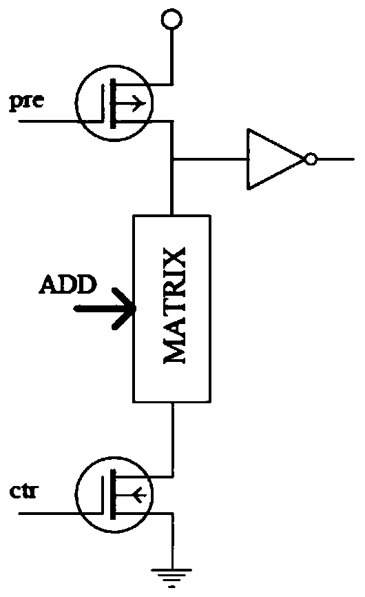
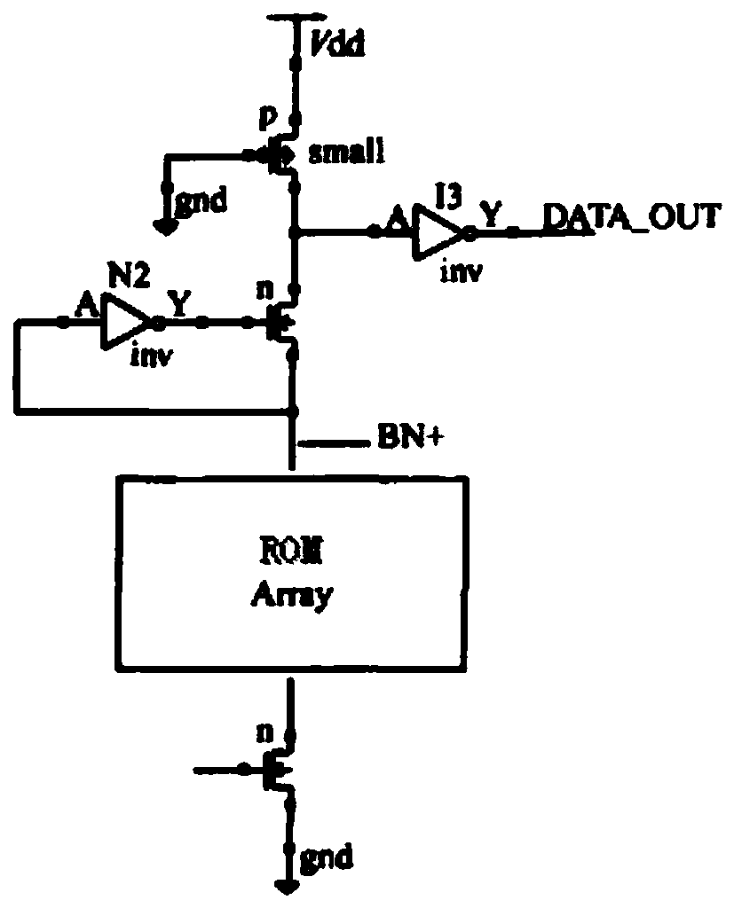
[0041] see Figure 6 to Figure 10 A readout structure of a mask memory according to a preferred embodiment of the present invention includes a MOS transistor P1 whose gate is connected to the PRE signal terminal, a MOS transistor N1 whose gate is connected to Vctrl, and the source of the MOS transistor N1 passes through the node RO Connected with the MaskROM storage array, the drain of MOS transistor N1 is connected to the drain of MOS transistor P1 to form node Net1, the source of MOS transistor P1 is connected to the power supply, and the readout structure of the mask memory also includes MOS transistor P2, MOS transistor P4, MOS transistor N2, MOS transistor N3, invert...


PUM


Abstract

The invention relates to a reading structure of a mask memory. By adopting a reasonable circuit structure, voltage reaching an adjacent BN + in a storage array is not more than 1V within the voltage range of a ROM working power supply of 2.2-5V, and the voltage is not related to factors such as ROM processing technology and layout of the ROM, so that N tubes in the storage array cannot be penetrated. When a reading structure of the mask memory is used for reading data, the reading is safe and accurate, the speed is high, and the power consumption is low.

Description

technical field [0001] The invention relates to a readout structure of a memory, in particular to a readout structure of a mask memory. Background technique [0002] An integrated circuit usually includes a read only memory (ROM, Read Only Memory) for storing fixed data and program codes. Read-only memory is a type of memory that can only read stored information during work, but cannot write information. The read-out information is stored in it in advance. ROMs are generally divided into two types: fixed ROMs and programmable ROMs / electrically erasable ROMs, and the present invention is mainly aimed at this type of fixed ROMs. The storage content of this kind of memory has been completely fixed when it leaves the factory, and it is programmed with a custom mask when the chip is made, so it is also called mask memory (Mask ROM). If you want to change the content in the ROM, you must Redoing the mask plate is more suitable for memory types with a large volume and a single pr...

Claims


Application Information

Patent Timeline
Patent Type & Authority Applications(China)
IPC IPC(8): G11C17/12G11C7/10
CPCG11C7/1048G11C7/106G11C17/12
Inventor 居水荣
Owner JIANGSU HAIDONG SEMICON TECH CO LTD
Why Eureka
Try Eureka