

Multi-layer chip structure and connecting method
A multi-layer chip and connection method technology, which is applied in the manufacture of electrical components, electrical solid devices, semiconductor/solid devices, etc., to achieve the effects of precise process positioning, accurate interconnection, and easy alignment
- Summary
- Abstract
- Description
- Claims
- Application Information
AI Technical Summary
Problems solved by technology
Method used
Image

Examples
Embodiment Construction
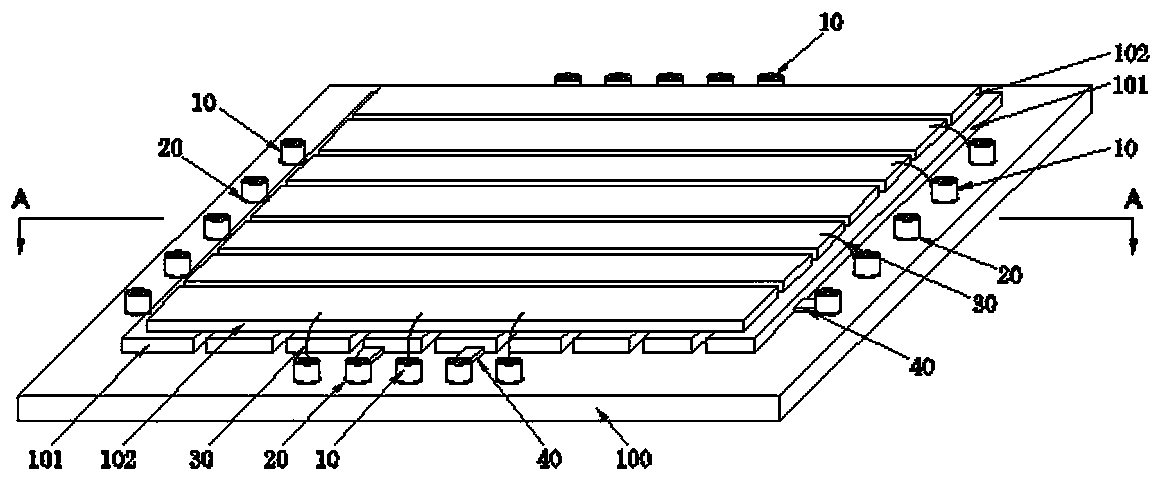
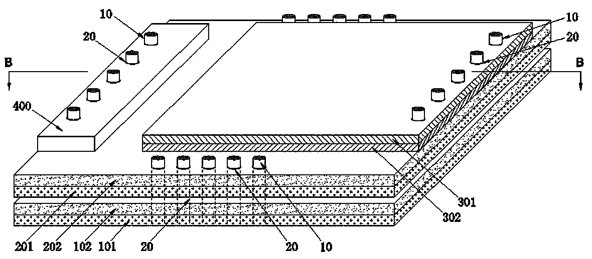
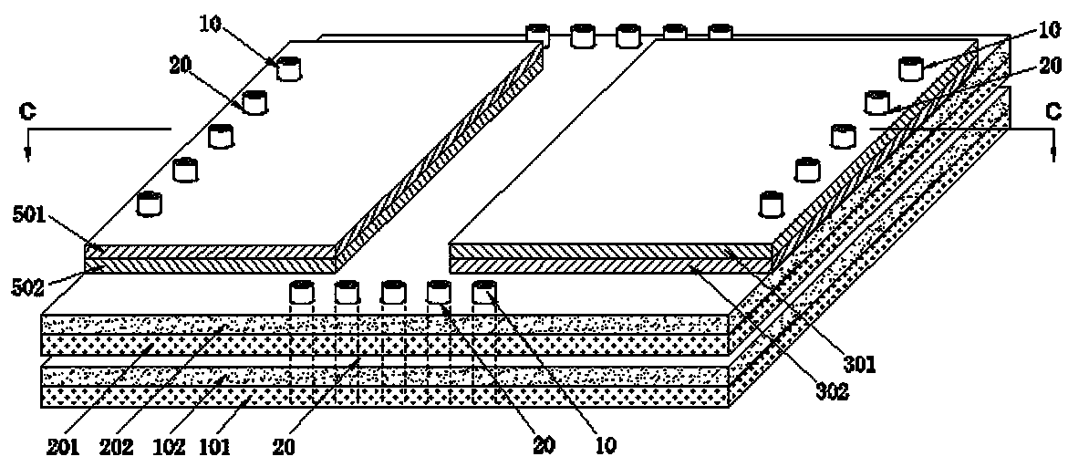
[0041] In a specific embodiment of the present invention, a multi-layer chip in a package includes chips of different geometric dimensions and different functionalized module chips, and a stack of conductive layers and auxiliary layers. In the implementation manner, each layer of stacked chips is arranged at the same position and at least in one direction, through silicon vias for interconnection between chip layers are laid out. The chip implementation of this multi-layer structure can provide optimized circuit design, layout of devices on the chip and wiring for improving electrical connection performance, as well as alignment of through-silicon holes between layers in the manufacturing process and positioning control of metal interconnection processes. The implementation of the present invention is specifically described and explained in detail as follows:
[0042] refer to figure 1 , the method of embodiment 1 includes a schematic diagram of chip architecture and position...
PUM
 Abstract
Description
Claims
Application Information