Supercharge Your Innovation With Domain-Expert AI Agents!

Device and method for cutting crystal rod

A technology for cutting devices and ingots, which is applied to fine working devices, stone processing equipment, manufacturing tools, etc. It can solve problems such as high defect rate, large deviation of silicon block crystal orientation, and poor surface quality of silicon wafers. Achieve the effect of improving quality, improving stability, and improving cutting quality

Active Publication Date: 2019-07-30
西安奕斯伟材料科技股份有限公司 +1
View PDF13 Cites 10 Cited by
  • Summary
  • Abstract
  • Description
  • Claims
  • Application Information

AI Technical Summary

Problems solved by technology

[0003] In view of this, the present invention provides a cutting device and a method for cutting crystal rods, which are used to solve the large deviation of the crystal orientation angle of the silicon block during cutting, which will easily lead to poor surface quality of the cut silicon chips. The problem of high defect rate

Method used


Image

  • Device and method for cutting crystal rod
  • Device and method for cutting crystal rod
  • Device and method for cutting crystal rod

Examples


Embodiment Construction

[0043] In order to make the purpose, technical solutions and advantages of the embodiments of the present invention more clear, the following will clearly and completely describe the technical solutions of the embodiments of the present invention in conjunction with the drawings of the embodiments of the present invention. Apparently, the described embodiments are some, not all, embodiments of the present invention. All other embodiments obtained by those skilled in the art based on the described embodiments of the present invention belong to the protection scope of the present invention.

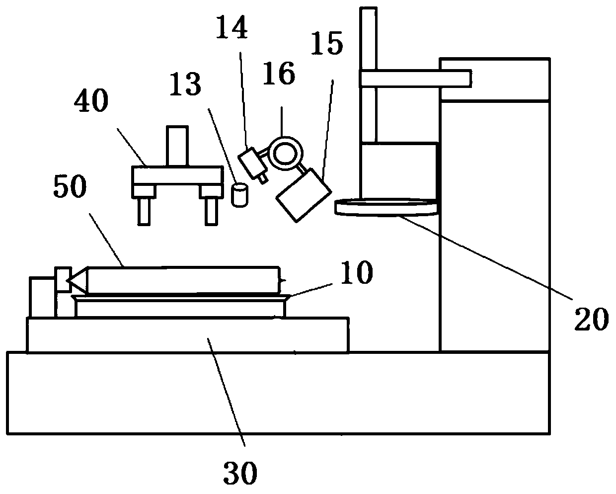
[0044] The cutting device according to the embodiment of the present invention will be described in detail below with reference to the accompanying drawings.

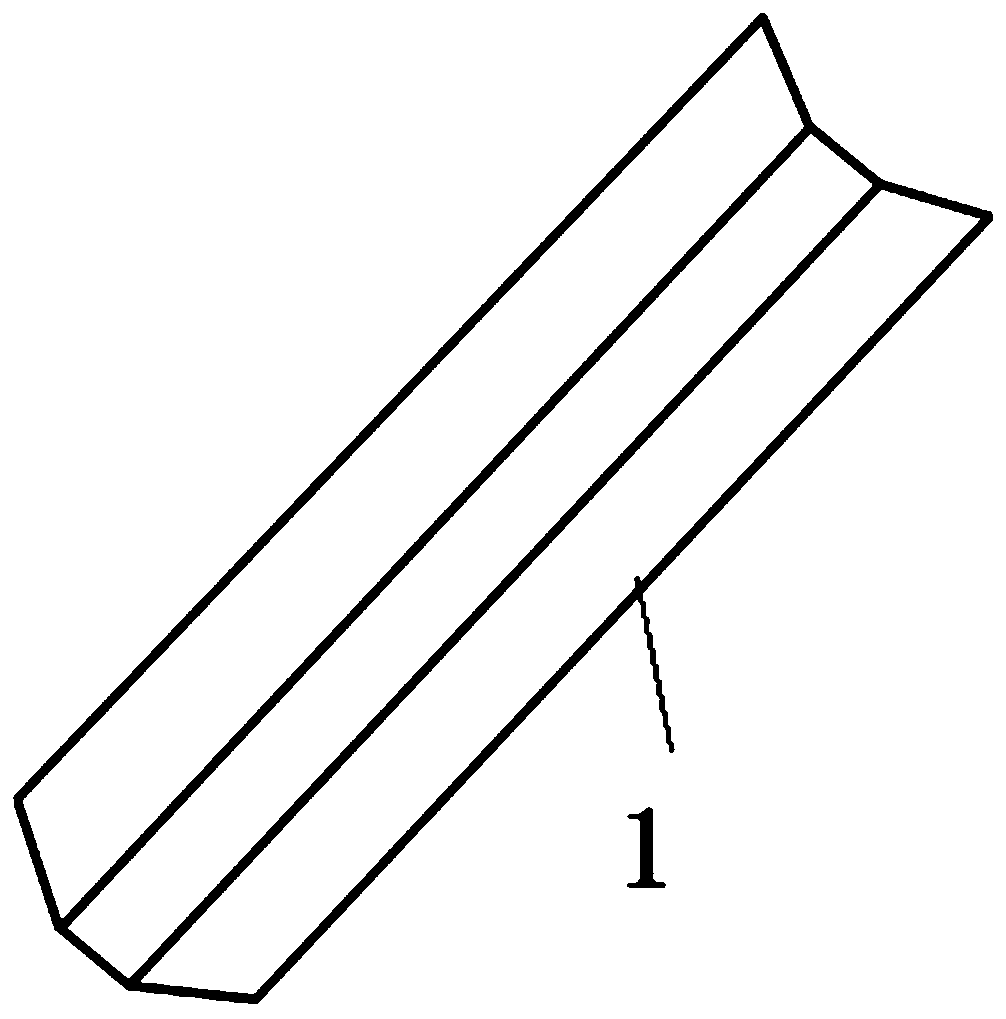
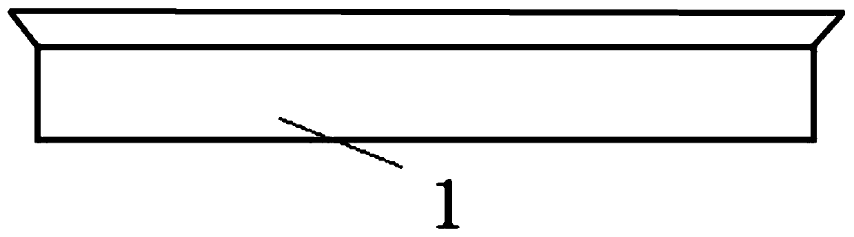
[0045] Such as figure 1 As shown, the cutting device according to the embodiment of the present invention includes: a carrying table 10 for carrying the crystal ingot 50 to be cut, and the carrying table 10 is provided with an adjus...


PUM


Abstract

The invention provides a device and method for cutting a crystal rod. The cutting device comprises a bearing platform, a detection mechanism, a cutting mechanism, a moving mechanism and a control mechanism, wherein the bearing platform is used to carry the crystal rod to be cut, and an adjusting mechanism for rotating and / or deflecting the crystal rod is arranged on the bearing platform; the detection mechanism is used to detect a crystal orientation deviation angle of the crystal rod; the cutting mechanism is used to cut the crystal rod; the moving mechanism is used to move the bearing platform; and the control mechanism is used to control the adjusting mechanism to adjust the crystal rod to a preset crystal orientation deviation angle according to a detection result and the cutting mechanism to cut the crystal rod after the crystal rod is moved to a preset position by moving the bearing mechanism by the moving mechanism. The crystal orientation deviation angle of the crystal rod is adjusted by the adjusting mechanism according to the cutting device, and the crystal rod is adjusted to the preset crystal orientation deviation angle according to the detection result, so that the cutting surface of a silicon block is perpendicular to the physical crystal orientation; and then the cutting mechanism is controlled to cut the crystal rod, so that the cutting quality is improved, thesurface quality of silicon wafers when the silicon block is cut into the silicon wafers is improved, and the situation that the crystal orientation deviation angle of the silicon block is within a control range during cutting the silicon block is ensured.

Description

technical field [0001] The invention relates to the field of silicon chip processing, in particular to a cutting device and a cutting method for crystal rods. Background technique [0002] Semiconductor devices are signal or energy control and conversion devices prepared by various processes on single crystal silicon wafers with the same crystal orientation. The crystal orientation of a single crystal silicon wafer is an important indicator for controlling the performance of a semiconductor, and it is generally required that the angle between the physical crystal orientation of the silicon wafer and the geometric central axis of the silicon wafer be controlled within ±0.5°. At present, the processing process for large-sized ingots above 8 inches is as follows: ingot rounding (ingot surface treatment), V-groove opening, band saw cutting (cutting ingots into silicon blocks), silicon block orientation orientation Bonding, multi-wire cutting (cutting silicon blocks into silicon...

Claims


Application Information

Patent Timeline
IPC IPC(8): B28D5/00B28D5/04
CPCB28D5/045B28D5/0058B28D5/0064
Inventor 兰洵全铉国陈光林
Owner 西安奕斯伟材料科技股份有限公司
Features
  • R&D
  • Intellectual Property
  • Life Sciences
  • Materials
  • Tech Scout
  • Unparalleled Data Quality
  • Higher Quality Content
  • 60% Fewer Hallucinations
Learn More