Spiral inductance optimization method based on HPSO algorithm and GA-BP algorithm

A GA-BP, spiral inductance technology, applied in the field of wireless communication, can solve the problems of inconvenient inductance optimization, time-consuming, increasing design cost, etc., to avoid falling into local extreme points and improve prediction accuracy.

Pending Publication Date: 2019-07-30
HUNAN UNIV
View PDF1 Cites 7 Cited by
  • Summary
  • Abstract
  • Description
  • Claims
  • Application Information

AI Technical Summary

Problems solved by technology

However, the current lack of fast and accurate computer-aided design (CAD) tools is one of the bottlenecks in RF circuit design. In traditional modeling techniques, numerical methods such as solving algebraic and differential equations can obtain accurate results for on-chip inductors, but require It takes too much time and increases the design cost. Analysis and empirical modeling techniques can effectively save time, but the calculation accuracy is not accurate enough, and some model calculation methods are not convenient for inductance optimization.

Method used


Image

  • Spiral inductance optimization method based on HPSO algorithm and GA-BP algorithm
  • Spiral inductance optimization method based on HPSO algorithm and GA-BP algorithm
  • Spiral inductance optimization method based on HPSO algorithm and GA-BP algorithm

Examples


Embodiment Construction

[0032] In order to illustrate the technical solution of the present invention more clearly, the present invention will be further described below in conjunction with the accompanying drawings and embodiments. It should be understood that the specific embodiments described here are only used to explain the present invention, not to limit the present invention.

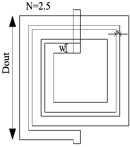
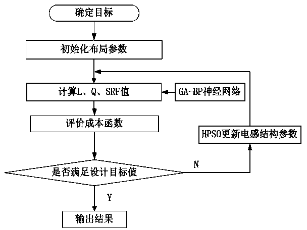
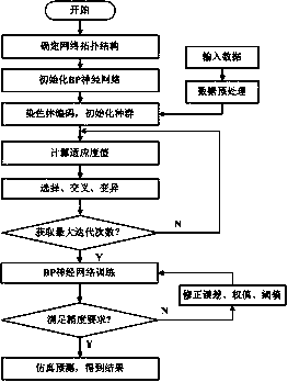
[0033] The method for optimizing the spiral inductance on the radio frequency chip based on the HPSO and GA-BP algorithm proposed by the present invention, its modeling flow chart is as follows figure 1 As shown, the following steps are included: Step 101. Make a data set: According to the 0.13-μm CMOS process technology, determine the structural parameters of the on-chip spiral inductor, that is, the number of turns N, the outer diameter Dout, the line width W, and the value range of the line spacing s as shown in Table 1 As shown, this range covers the potential inductor size of a typical wireless communication applic...


PUM


Abstract

The invention discloses a spiral inductance optimization method based on HPSO algorithm and GA-BP algorithm. The spiral inductance optimization method comprises the steps that an on-chip spiral inductance data set is manufactured through electromagnetic simulation software HFSS, and data preprocessing is carried out; a genetic algorithm (GA) is adopted to optimize the BP neural network, then the optimized BP neural network is trained, and a GA-BP model is established; layout search is performed on the on-chip spiral inductor by adopting HPSO to obtain structure parameters meeting constraint conditions under a specific target inductance value; characterization parameter prediction is carried out on the structure parameters of the on-chip spiral inductor under the specific inductance value by using the GA-BP model. The method can help designers compromise and analyze the inductive performance and the inductive size, enables the circuit to have the optimal performance and the optimal size, not only guarantees the accuracy of the calculation result, but also can save time and cost, and has a good application prospect.

Description

technical field [0001] The invention relates to a spiral inductance optimization method based on HPSO and GA-BP algorithms, which belongs to the field of wireless communication. Background technique [0002] With the rapid development of wireless communication, the design requirements of radio frequency devices are getting higher and higher. The on-chip spiral inductor is a key component of the radio frequency circuit. The quality factor Q value is an extremely important parameter of the on-chip inductor. The higher the Q value of the inductor, the smaller the loss and the higher the efficiency; the high-Q on-chip inductor is easy to integrate and extremely Flexibility is suitable for the requirements of low-loss and low-cost devices in the modern radio frequency and microwave field, and is of great significance for achieving high-performance filtering, tuning, and amplification. However, the current lack of fast and accurate computer-aided design (CAD) tools is one of the ...

Claims


Application Information

Patent Timeline
Patent Type & Authority Applications(China)
IPC IPC(8): G06F17/50G06N3/00G06N3/04G06N3/08
CPCG06N3/086G06N3/006G06F30/36G06F30/20G06N3/044
Inventor 杜四春欧伟黎赛银红霞
Owner HUNAN UNIV
Why Eureka
Try Eureka