Three-dimensional NAND type ferroelectric memory, manufacturing method and operation method

A ferroelectric memory, a three-dimensional technology, applied in the field of memory, can solve the problems of reducing the storage window, limiting the reading speed, and increasing leakage, and achieves the effects of increasing the storage window, improving reliability, and reducing the electric field

Active Publication Date: 2019-07-30
INST OF MICROELECTRONICS CHINESE ACAD OF SCI
View PDF6 Cites 7 Cited by
  • Summary
  • Abstract
  • Description
  • Claims
  • Application Information

AI Technical Summary

Problems solved by technology

[0003] However, based on the traditional hafnium-based ferroelectric memory, the charge trapping of the ferroelectric layer during the erasing and writing process will neutralize the polarization reversal of the ferroelectric layer, thereby making its storage window smaller; the release process of the charge trapped by the ferroelectric layer It will also affect the reading operation after erasing and writing, thereby limiting the reading speed; and, the unreasonable distribution of the electric field in the ferroelectric layer and the dielectric layer reduces the electric field between the two sides of the ferroelectric layer on the one hand, causing the device to work In the ferroelectric unsaturated region, the storage window is reduced, and on the other hand, the electric field on both sides of the dielectric layer is too large, resulting in increased leakage and reduced durability.

Method used


Image

  • Three-dimensional NAND type ferroelectric memory, manufacturing method and operation method
  • Three-dimensional NAND type ferroelectric memory, manufacturing method and operation method
  • Three-dimensional NAND type ferroelectric memory, manufacturing method and operation method

Examples


Embodiment Construction

[0045] The following will clearly and completely describe the technical solutions in the embodiments of the present invention with reference to the accompanying drawings in the embodiments of the present invention. Obviously, the described embodiments are only some, not all, embodiments of the present invention. Based on the embodiments of the present invention, all other embodiments obtained by persons of ordinary skill in the art without making creative efforts belong to the protection scope of the present invention.

[0046] In order to make the above objects, features and advantages of the present invention more comprehensible, the present invention will be further described in detail below in conjunction with the accompanying drawings and specific embodiments.

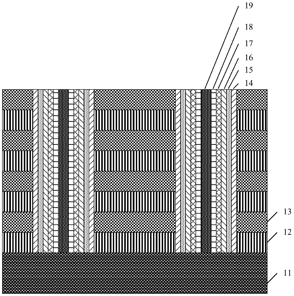
[0047] refer to figure 1 , figure 1 A schematic structural diagram of a three-dimensional NAND ferroelectric memory provided by an embodiment of the present invention, the three-dimensional NAND ferroelectric mem...


PUM


Abstract

The invention provides a three-dimensional NAND type ferroelectric memory, a manufacturing method and an operation method; the three-dimensional NAND type ferroelectric memory takes the inherent electric field adjusting effect of a ring gate device into consideration, namely compared with a flat-plate laminated gate, in a ring gate dielectric laminated layer, the electric field is enhanced in thedielectric layer with small radius and the electric field is weakened in the dielectric layer with large radius; a ferroelectric layer is integrated on the small-radius inner ring of the ring gate, and a dielectric layer is integrated on the outer ring of the large radius, so that the electric field distribution is effectively adjusted, the electric field of the dielectric layer is reduced, and the electric field of the ferroelectric layer is enhanced, and therefore the reliability of the ferroelectric memory is effectively improved, namely, the storage window is enlarged, the durability of the device is improved, and the retention characteristic of the device is improved.

Description

technical field [0001] The invention relates to the technical field of memory, more specifically, to a three-dimensional NAND type ferroelectric memory, a manufacturing method and an operating method. Background technique [0002] Currently, the use of ferroelectric transistors as nonvolatile memories has attracted extensive research by researchers due to the breakthrough in ferroelectricity research on doped hafnium-based materials. Among them, hafnium-based ferroelectric memory has the advantages of easy scaling and compatibility with traditional CMOS technology. [0003] However, based on the traditional hafnium-based ferroelectric memory, the charge trapping of the ferroelectric layer during the erasing and writing process will neutralize the polarization reversal of the ferroelectric layer, thereby making its storage window smaller; the release process of the charge trapped by the ferroelectric layer It will also affect the reading operation after erasing and writing, ...

Claims


Application Information

Patent Timeline
Patent Type & Authority Applications(China)
IPC IPC(8): H01L27/11597G11C11/22
CPCG11C11/2275G11C11/2273H10B51/20
Inventor 李春龙霍宗亮张瑜洪培真邹兴奇靳磊
Owner INST OF MICROELECTRONICS CHINESE ACAD OF SCI
Why Eureka
Try Eureka