Apparatuses and methods for calibrating adjustable impedances of a semiconductor device

A semiconductor and equipment technology, which is applied to equipment and fields for calibrating the adjustable impedance of semiconductor devices, and can solve problems such as impracticality

Active Publication Date: 2019-07-30
MICRON TECH INC
View PDF10 Cites 1 Cited by
  • Summary
  • Abstract
  • Description
  • Claims
  • Application Information

AI Technical Summary

Problems solved by technology

At some point, it is not practical to complete the calibration operation of all the devices of the system within the specified time

Method used


Image

  • Apparatuses and methods for calibrating adjustable impedances of a semiconductor device
  • Apparatuses and methods for calibrating adjustable impedances of a semiconductor device
  • Apparatuses and methods for calibrating adjustable impedances of a semiconductor device

Examples


Embodiment Construction

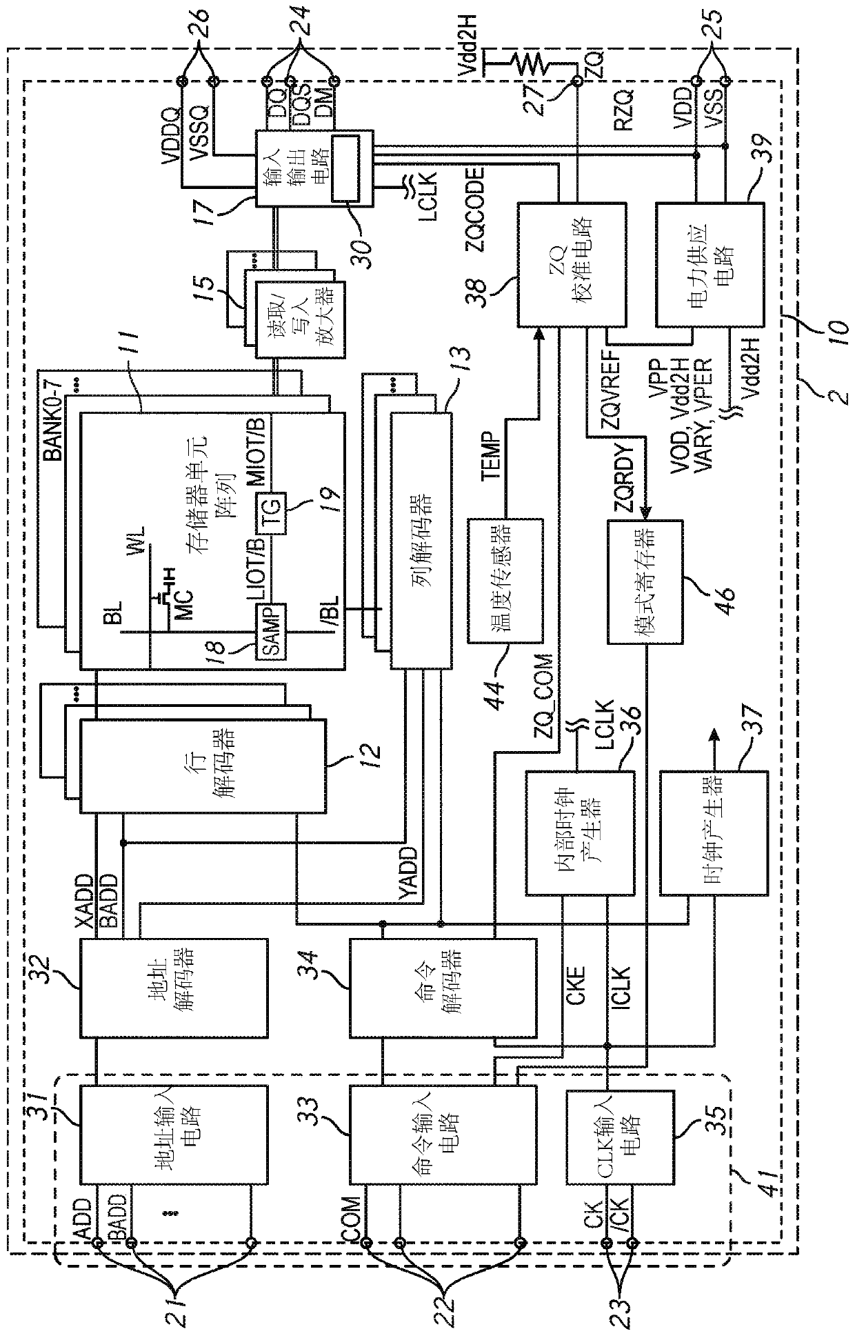
[0024] Specific details are set forth below in order to provide a thorough understanding of embodiments of the invention. It will be apparent, however, to one skilled in the art that embodiments of the invention may be practiced without these specific details. Furthermore, the specific embodiments of the invention described herein are provided by way of example and should not be used to limit the scope of the invention to these specific embodiments. In other instances, well-known circuits, control signals, timing protocols and software operations have not been shown in detail to avoid unnecessarily obscuring the present invention.

[0025] figure 1 is a block diagram of a semiconductor device 10 according to an embodiment of the present invention. The semiconductor device 10 may be a DDR5 SDRAM integrated into, for example, a single semiconductor chip. The semiconductor device 10 may be mounted on an external substrate 2 which is a memory module substrate, a motherboard, o...


PUM


Abstract

Apparatuses and methods for calibrating adjustable impedances of a semiconductor device are disclosed in the present application. An example apparatus includes a register configured to store impedancecalibration information and further includes programmable termination resistances having a programmable impedance. The example apparatus further includes an impedance calibration circuit configured to perform a calibration operation to determine calibration parameters for setting the programmable impedance of the programmable termination resistances. The impedance calibration circuit is further configured to program the impedance calibration information in the register related to the calibration operation.

Description

[0001] Cross References to Related Applications [0002] This application claims the benefit of U.S. Provisional Application No. 62 / 432,494, filed December 9, 2016. This application is hereby incorporated by reference in its entirety and for all purposes. Background technique [0003] Semiconductor devices such as microcomputers, memories, gate arrays, and the like include input / output pins and output circuits for transmitting data to other devices via buses, transmission lines formed on a board, and the like. Circuits within a semiconductor device responsible for transferring data include, for example, output buffers and drivers. For optimal transmission, the impedance of the transmitting device should match the impedance of the transmission network and the receiving device. [0004] As the operating speed of electronic devices increases, the swing of transmission signals decreases. However, as the signal swing width of the transmission signal decreases, external noise in...

Claims


Application Information

Patent Timeline
Patent Type & Authority Applications(China)
IPC IPC(8): G11C7/10
CPCG11C29/025G11C29/028G11C29/022G11C2029/4402G11C29/16G11C7/1057G11C7/1084G11C2029/0409G11C7/1048G11C2207/2254H03H11/54H03H11/28G11C7/10H03K19/0005
Inventor D·甘斯
Owner MICRON TECH INC
Why Eureka
Try Eureka