Unlock instant, AI-driven research and patent intelligence for your innovation.
An ultrasonic-assisted pillar planting method for cucga device packaging
What is Al technical title?
Al technical title is built by PatSnap Al team. It summarizes the technical point description of the patent document.
An ultrasonic-assisted and device packaging technology, which is applied to the assembly of printed circuits with electrical components, electrical solid devices, semiconductor devices, etc., can solve the problem of solder joint porosity and solder post scratch damage, large impact on the quality of planted posts, and welding heat transfer. Bad and other issues
Active Publication Date: 2020-12-25
HARBIN UNIV OF SCI & TECH
View PDF1 Cites 0 Cited by
Summary
Abstract
Description
Claims
Application Information
AI Technical Summary
This helps you quickly interpret patents by identifying the three key elements:
Problems solved by technology
Method used
Benefits of technology
Problems solved by technology
[0006] The present invention aims to solve the problems that the post-planting of arrayed copper pillars in the existing CuCGA device package is difficult, the quality of the post-planting is greatly affected by the auxiliary mold, and it is prone to poor welding heat transfer, solder joint pores and solder post scratches and damages, etc.
Method used
Image
Click on the blue label to locate the original text in one second.
Reading with bidirectional positioning of images and text.
Examples
specific Embodiment approach 1
[0044]An ultrasonic assisted pillar planting method for CuCGA device packaging includes the following steps:
[0045]Step 1. Print solder paste with non-eutectic point solder composition on the pads arranged in the array:
[0046]Same as the traditional BGA ball planting process, a sufficient amount of non-eutectic point solder composition solder paste is printed on the pads arranged in the array of the printed circuit board and the chip carrier substrate by means of a mature stencil printing process;
[0047]Step 2. Realize the ball planting on the pads arranged in the array on the printed circuit board and the chip carrier substrate by reflow soldering:
[0048]The solder paste on the pads arranged in an array on the printed circuit board and the chip carrier substrate is heated to melt, the flux in the solder paste removes the oxide film on the pads, and the solder in the solder paste wets the pads, and The solder balls arranged in an array are formed under the action of surface tension;
[004...
specific Embodiment approach 2
[0059]The material of the pads arranged in the array in this embodiment is any one of copper, gold, silver, nickel, tin bronze, brass, or a combination of copper, gold, silver, nickel, tin bronze, or brass The multilayer metal film pad formed by the combination may also be one of the metals or alloys on which other tin-based solders can be well wetted.
[0060]The other steps and parameters are the same as in the first embodiment.
specific Embodiment approach 3
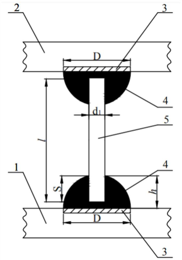
[0062]The diameter of the pads arranged in the array according to this embodiment is D, 0.9mm≦D≦3mm, and the thickness of the pads arranged in the array is 35 μm-100 μm.
[0063]The other steps and parameters are the same as in the first or second embodiment.
PUM
Property
Measurement
Unit
thickness
aaaaa
aaaaa
length
aaaaa
aaaaa
diameter
aaaaa
aaaaa
Abstract
The invention relates to an ultrasound-assisted column implanting method for CuCGA (Ceramic Copper Column Grid Array) device packaging, and relates to the technical field of microelectronic packaging.The invention aims to solve a problem that the column implanting quality of devices is easy to be affected by assistant dies and has poor heat transfer, welding spot porosity and welding column scratches in the traditional method. The method comprises the steps of printing soldering paste with non-eutectic point solder components on welding pads arrayed in an array mode of a chip carrier substrate and a printed circuit board, and realizing solder sphere placement on the bonding pad through reflow soldering; then forming positioning holes with the same size in the arrayed solder spheres; and inserting copper columns with the same specifications into the positioning holes of the solder spheres arranged in an array mode at two ends of the substrate, and achieving double-sided implantation connection of the arrayed copper columns by adopting an ultrasound-assisted solid-liquid coexistence zone solder reflow soldering method. Ultrasound cavitation can promote the destruction of an oxide film on the surface of the copper column, the micro-flow of the solder and the inter-diffusion of interfacial atoms, and can refine the solder structure, reduce the porosity and improve the joint strength. The ultrasound-assisted column implanting method is applied to CuCGA device column implanting without being die assistance.
Description
Technical field[0001]The invention relates to the technical field of microelectronic packaging, in particular to an ultrasonic assisted pillar planting method for CuCGA device packaging.Background technique[0002]In the area array package, the CuCGA (Ceramic Copper Column Grid Array) package has a higher height and greater flexibility than the CBGA (Ceramic Ball Grid Array) package. It has better heat dissipation capability and can use copper The flexural deformation of the column effectively releases the internal stress of the interconnection structure, so it has a higher thermal cycle life. CuCGA packaging is widely used in high-frequency, high-power, high-I / O large chip packaging and high-reliability requirements for aviation, aerospace, and military electronic devices.[0003]The process in which the copper pillars are arranged in an array and vertically connected to the pads arranged in the array is called pillar planting. However, the large aspect ratio and poor stability of copp...
Claims
Application Information
Patent Timeline
Application Date:The date an application was filed.
Publication Date:The date a patent or application was officially published.
First Publication Date:The earliest publication date of a patent with the same application number.
Issue Date:Publication date of the patent grant document.
PCT Entry Date:The Entry date of PCT National Phase.
Estimated Expiry Date:The statutory expiry date of a patent right according to the Patent Law, and it is the longest term of protection that the patent right can achieve without the termination of the patent right due to other reasons(Term extension factor has been taken into account ).
Invalid Date:Actual expiry date is based on effective date or publication date of legal transaction data of invalid patent.
