Unlock instant, AI-driven research and patent intelligence for your innovation.

Semiconductor packaging structure and manufacturing method thereof

A packaging structure and semiconductor technology, which is applied in semiconductor/solid-state device manufacturing, semiconductor devices, semiconductor/solid-state device components, etc., can solve the problems of low integration of antenna packaging structure, complicated preparation process, and high preparation cost, and achieve economical preparation Effects of cost, simplification of preparation process, reduction in size and volume

Pending Publication Date: 2019-08-02
SJ SEMICON JIANGYIN CORP
View PDF0 Cites 5 Cited by
  • Summary
  • Abstract
  • Description
  • Claims
  • Application Information

AI Technical Summary

Problems solved by technology

[0005] In view of the above-mentioned shortcomings of the prior art, the purpose of the present invention is to provide a semiconductor packaging structure and its preparation method, which is used to solve the problem of low integration, large size, complicated preparation process and preparation method of the antenna packaging structure in the prior art. high cost issues

Method used


Image

  • Semiconductor packaging structure and manufacturing method thereof
  • Semiconductor packaging structure and manufacturing method thereof
  • Semiconductor packaging structure and manufacturing method thereof

Examples


Embodiment 1

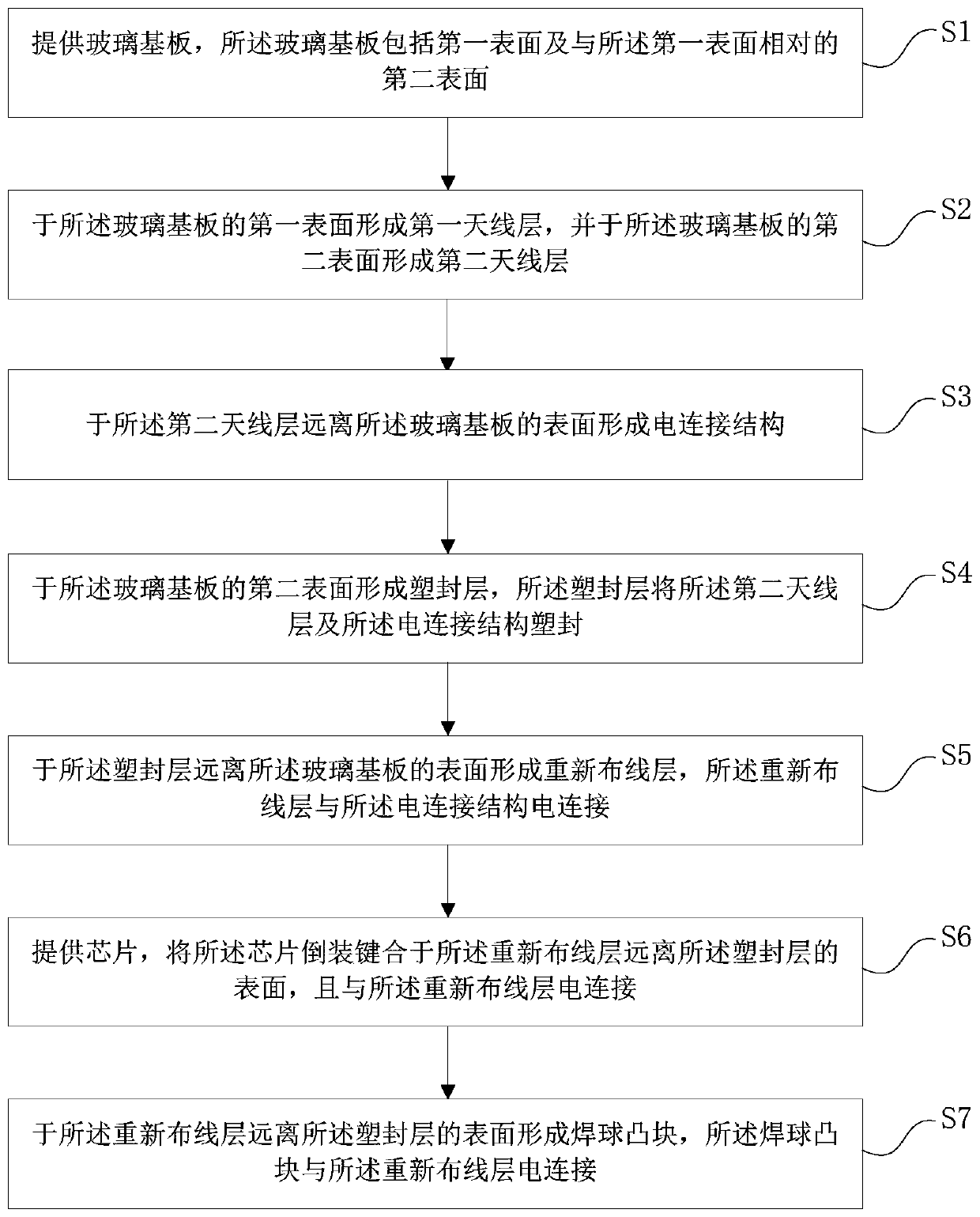
[0056] see figure 1 , the invention provides a method for preparing a semiconductor package structure, the method for preparing a semiconductor package structure includes the following steps:

[0057] 1) providing a glass substrate, the glass substrate comprising a first surface and a second surface opposite to the first surface;

[0058] 2) forming a first antenna layer on the first surface of the glass substrate, and forming a second antenna layer on the second surface of the glass substrate;

[0059] 3) forming an electrical connection structure on the surface of the second antenna layer away from the glass substrate;

[0060] 4) forming a plastic seal layer on the second surface of the glass substrate, and the plastic seal layer seals the second antenna layer and the electrical connection structure;

[0061] 5) forming a rewiring layer on the surface of the plastic sealing layer away from the glass substrate, and the rewiring layer is electrically connected to the electr...

Embodiment 2

[0099] Please combine Figure 2 to Figure 8 refer to Figure 9 , the present invention also provides a semiconductor packaging structure, the semiconductor packaging structure comprising: a glass substrate 10, the glass substrate 10 includes a first surface and a second surface opposite to the first surface; a first antenna layer 11, The first antenna layer 11 is located on the first surface of the glass substrate 10; the second antenna layer 12, the second antenna layer 12 is located on the second surface of the glass substrate 10; the electrical connection structure 13, the electrical The connection structure 13 is located on the surface of the second antenna layer 12 away from the glass substrate 10; the plastic sealing layer 14, the plastic sealing layer 14 is located on the second surface of the glass substrate 10, and the plastic sealing layer 14 seals the first Two antenna layers 12 and the electrical connection structure 13 are plastic-encapsulated; a re-wiring layer ...


PUM


Abstract

The invention provides a semiconductor packaging structure and a manufacturing method thereof. The semiconductor packaging structure comprises a glass substrate, a first antenna layer, a second antenna layer, an electrical connection structure, a plastic packaging layer, a rewiring layer, a chip and a solder ball bump, wherein the glass substrate comprises a first surface and a second surface which are opposite; the first antenna layer is located on the first surface of the glass substrate; the second antenna layer is located on the second surface of the glass substrate; the electrical connection structure is located on the surface, far away from the glass substrate, of the second antenna layer; the plastic packaging layer is located on the second surface of the glass substrate; the rewiring layer is located on the surface, far away from the glass substrate, of the plastic packaging layer, and the rewiring layer is electrically connected with the electrical connection structure; the chip is flip bonded on the surface, far away from the plastic packaging layer, of the rewiring layer and is electrically connected with the rewiring layer; and the solder ball bump is located on the surface, far away from the plastic packaging layer, of the rewiring layer and is electrically connected with the rewiring layer. The semiconductor packaging structure can significantly narrow reduce thesize and the volume of the semiconductor packaging structure and improves the integration degree of the device; no additional carrier is required for packaging transfer, which significantly simplifiesthe preparation process and saves the preparation cost.

Description

technical field [0001] The invention belongs to the field of semiconductor packaging, in particular to a semiconductor packaging structure and a preparation method thereof. Background technique [0002] With the development of the economy and the advancement of science and technology, various high-tech electronic products emerge in an endless stream, which greatly facilitates and enriches people's lives. Among them, the development of various portable mobile communication terminals represented by mobile phones and tablet computers (PAD) Especially eye-catching. [0003] Existing portable mobile communication terminals usually have a built-in antenna structure for communication functions, such as implementing voice and video connections and surfing the Internet. At present, the common method of building the antenna is to directly fabricate the antenna on the surface of the circuit board. However, due to the additional area of ​​the circuit board occupied by the antenna, the ...

Claims


Application Information

Patent Timeline
IPC IPC(8): H01L23/66H01L23/15H01Q1/22H01L21/48
CPCH01L23/66H01L23/15H01L21/4814H01Q1/2283H01L2224/73204H01L2224/16227H01L2224/32225H01L2924/15321H01L2223/6677H01L2224/16225H01L2924/00
Inventor 陈彦亨林正忠
Owner SJ SEMICON JIANGYIN CORP