Textured surfaces for polynucleotide synthesis
A technology of polynucleotides and nucleosides, applied in the direction of combinatorial chemistry, chemical libraries, and the introduction of foreign genetic materials using vectors, etc., which can solve the problems of scalability, automation, speed, accuracy, and cost.
- Summary
- Abstract
- Description
- Claims
- Application Information
AI Technical Summary
Problems solved by technology
Method used
Image
Examples
preparation example Construction
[0152] Provided herein are surface preparation methods in which photolithography is followed by a reactive chemical vapor deposition (CVD) step. Optionally, an exemplary first step includes cleaning the surface of the device using the cleaning methods disclosed herein. Cleaning may include oxygen plasma treatment. In some cases, a CVD step is used to deposit a mixture having at least two molecules resulting in regions of high surface energy and regions coated with a first chemical layer that is a region of lower surface energy. The mixture may comprise molecules bound to the surface and coupled to nucleoside phosphoramidites mixed with a larger number of molecules bound to the surface but not coupled to nucleoside phosphoramidites. For the two-step dilution scheme, prior to depositing the mixture on the surface, the step involves depositing 100% of the mixture constituent molecules that are bound to the surface but not conjugated to the nucleoside phosphoramidites. The first...
Embodiment 1
[0272] Example 1: Textured Silicon Array
[0273] An array of pillars is etched into a silicon dioxide wafer to increase the surface area by a factor of 2 to 3. Figure 18-21 An image of the microfluidic device is shown. Figure 18 and 19 is a top-view image of the microfluidic device. Figure 20 is a side-view image of the microfluidic device at 52 degrees, at a scale capable of distinguishing the pillars of the textured surface. Figure 21 is a side view of a textured microfluidic device.
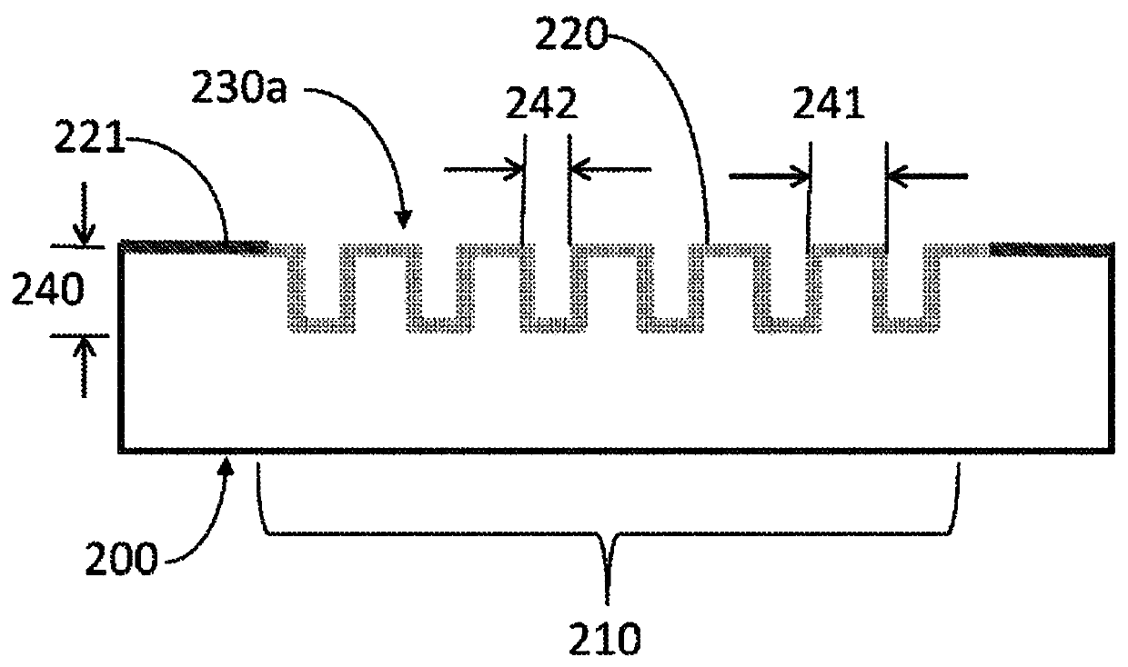
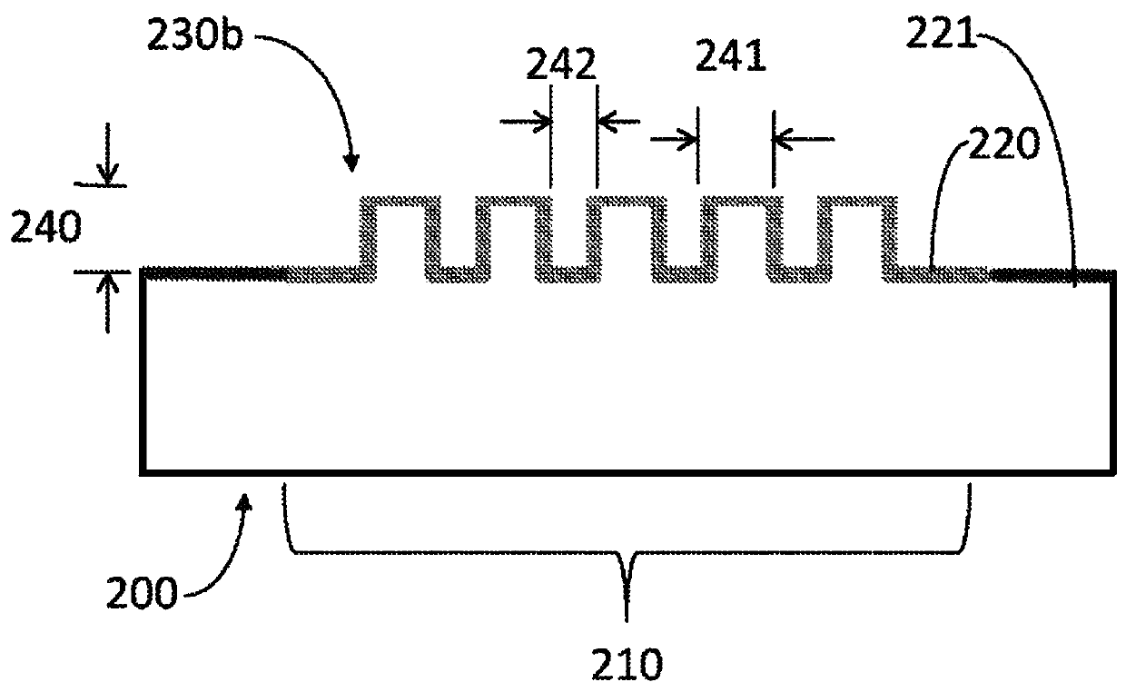
[0274] Textured silicon arrays were fabricated with the following characteristics: the measured height of the etched pillars was 746 nm, the width of the pillar tops was 272 nm, and the width of the pillar bottoms was 264 nm, and the thickness of the thermal oxide layer "capping" the pillars was 74nm.
[0275] Figures 22A-22B Additional images of the microfluidic device are shown. Figure 22A is a side-view image of the microfluidic device that highlights the macroscopic geometry ...
Embodiment 2
[0280] Example 2: Design, fabrication and analysis of arrays with textured loci for polynucleotide extension
[0281] array design. Silicon plates were fabricated with the following features designed for etched pillars: Array A: the height of the oxide "cap" at the top of the pillars was 122 nm; the etch depth of the pillars was 301 nm; and the pillar width at the bottom was 320 nm; and Array B: the top of the pillars The height of the oxide "cap" is 112 nm; the etch depth of the pillars is 426 nm; and the pillar width at the bottom is 316 nm.
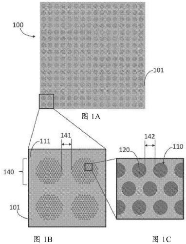
[0282] Synthesis on fabricated boards with textured seats. Each silicon plate contains an array of clusters, each cluster having a discrete position ("locus") for nucleotide extension. Figures 23A-23B Depicted are low magnification images of locus clusters after performing polynucleotide synthesis reactions. Figure 23A Image depicting clusters of non-textured loci. Figure 23B Images depicting clusters of textured loci.
[0283]...
PUM
| Property | Measurement | Unit |
|---|---|---|
| tensile strength | aaaaa | aaaaa |
| tensile strength | aaaaa | aaaaa |
| width | aaaaa | aaaaa |
Abstract
Description
Claims
Application Information


