
Multi-chip fan-out packaging structure with cavity and manufacturing method of multi-chip fan-out packaging structure

A packaging structure and multi-chip technology, applied in semiconductor/solid-state device manufacturing, electrical components, electrical solid-state devices, etc., can solve problems such as complex process, technical difficulty, and high cost, and achieve simplified process, reduced cost, and excellent electrical performance Effect

Pending Publication Date: 2019-08-23
XIAMEN SKY SEMICON TECH CO LTD
View PDF0 Cites 3 Cited by
  • Summary
  • Abstract
  • Description
  • Claims
  • Application Information

AI Technical Summary

Problems solved by technology

The main problems are: it is necessary to make corresponding characteristic graphics on the surface of the slide (set the chip placement area); use temporary bonding process and equipment; must use wafer-level injection molding equipment and process; must use debonding equipment and process
The existing fan-out process is complex, technically difficult, and costly, which limits its application

Method used


Image

  • Multi-chip fan-out packaging structure with cavity and manufacturing method of multi-chip fan-out packaging structure
  • Multi-chip fan-out packaging structure with cavity and manufacturing method of multi-chip fan-out packaging structure
  • Multi-chip fan-out packaging structure with cavity and manufacturing method of multi-chip fan-out packaging structure

Examples


Embodiment Construction

[0032] The present invention will be further described below through specific embodiments. The drawings of the present invention are only schematic diagrams for easier understanding of the present invention, and their specific proportions can be adjusted according to design requirements. The upper and lower relationship of the relative components in the figures described herein should be understood by those skilled in the art to refer to the relative positions of the components. Correspondingly, the upper side of the component is the front and the lower side is the back for easy understanding, so all The same components can be turned over to present, all of which should belong to the scope disclosed in this specification.

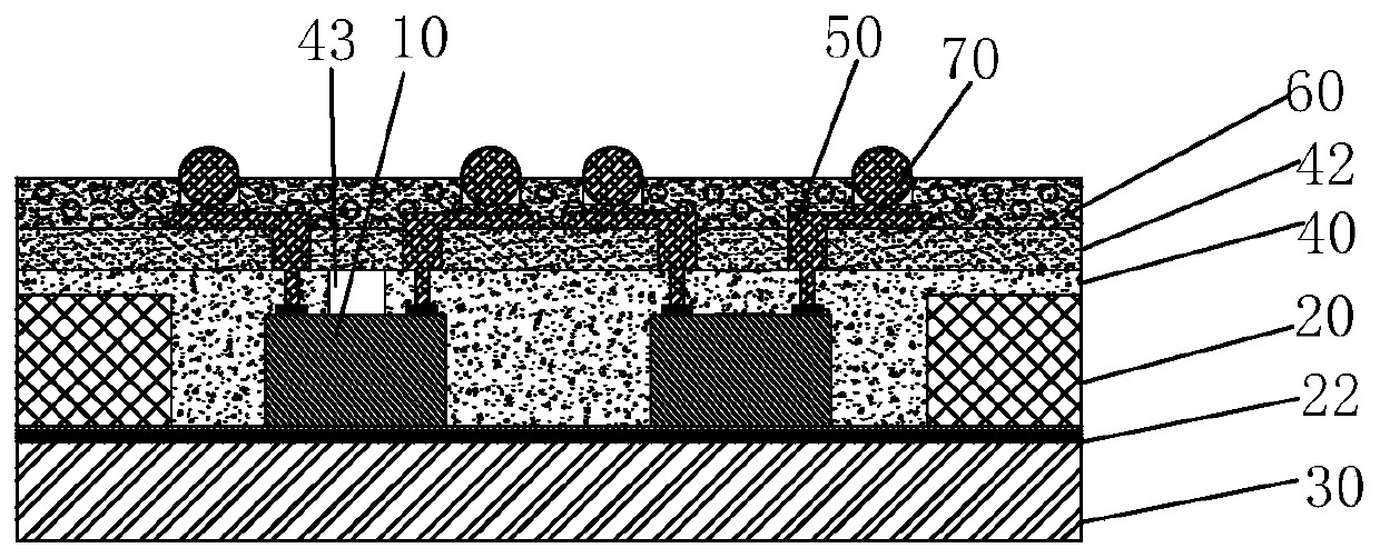
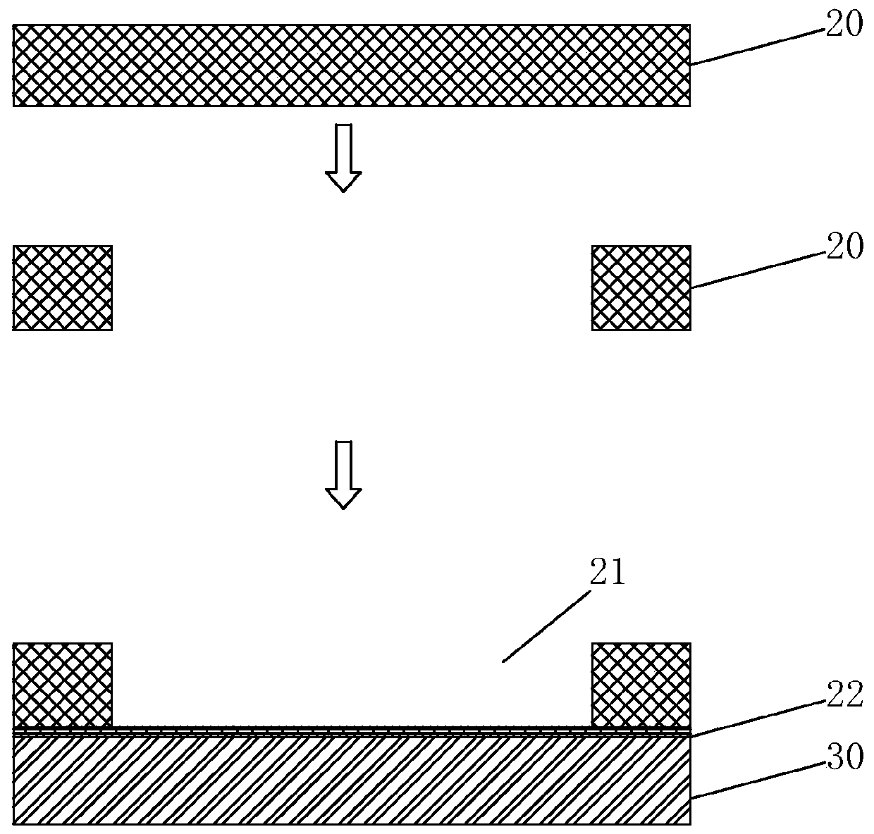
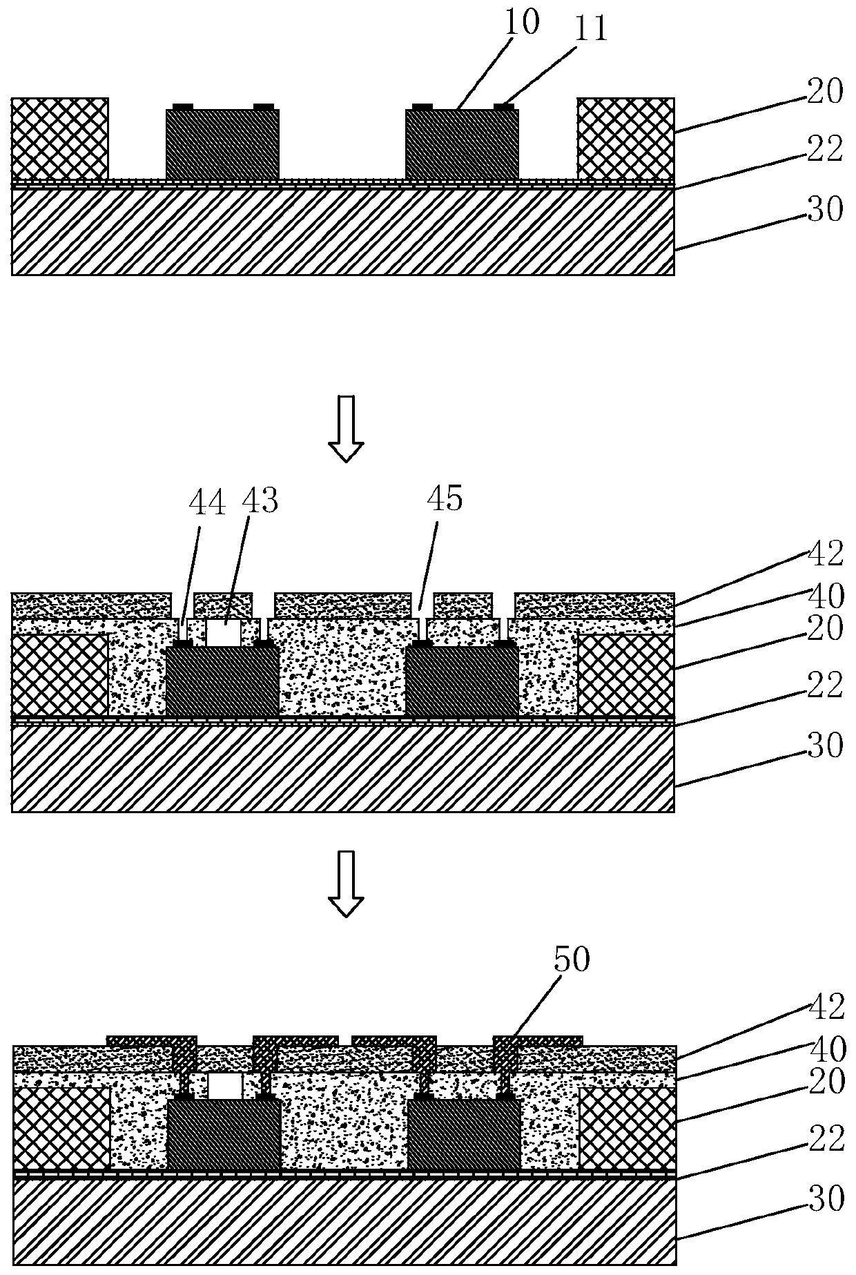
[0033] refer to figure 1 , a cavity-containing multi-chip fan-out packaging structure, including a chip 10, a first carrier 20, a second carrier 30, a filling layer 40, a metal rewiring layer 50, a first insulating layer 42, a second insulating layer 60 an...


PUM


Abstract

The invention relates to a multi-chip fan-out packaging structure with a cavity and a manufacturing method of the multi-chip fan-out packaging structure. The multi-chip fan-out packaging structure comprises at least two chips, and the first surface of each chip is provided with a bonding pad and a functional region. The multi-chip fan-out packaging structure also comprises a first carrier, a second carrier, a filling layer, a metal rewiring layer, a first insulating layer, a second insulating layer and a signal port. The first carrier is connected to the first surface of the second carrier andis provided with a through hole; the chip is located in the through hole, and the second surface of the chip is connected to the first surface of the first carrier; the filling layer covers the firstcarrier and the first surface of the chip and is provided with a first opening; the first insulating layer covers the surface of the filling layer, so that the cavity is formed in the functional area, and a second opening is formed in the bonding pad; the metal rewiring layer is positioned on the upper surface of the first insulating layer and is electrically connected with the bonding pad; the second insulating layer covers the surfaces of the first insulating layer and the metal rewiring layer and is provided with a third opening; and the signal port is located at the third opening and is electrically connected with the metal rewiring layer. The structure can improve the packaging reliability, is small in size, and reduces the cost.

Description

technical field [0001] The invention relates to the field of semiconductor packaging, in particular to a cavity-containing multi-chip fan-out packaging structure and a manufacturing method thereof. Background technique [0002] With the trend of multi-functionalization and miniaturization of electronic products, especially the development of smart phones, tablet computers, wearable devices and other products, chip functions are becoming more and more complex, chip size is getting smaller and smaller, and the number of I / Os is getting higher and higher. More and more, Fan-in (fan-in) packaging can no longer meet the requirements of I / O fan-out. Fan-out (fan-out) packaging technology is a supplement to fan-in packaging technology, and the chip I / O port is led out by reconfiguring the wafer. [0003] The fan-out process has been applied since 2008, mainly the eWLB (Embedded WaferLevel BGA) technology of Infineon Wireless. With the gradual maturity of process technology and th...

Claims


Application Information

Patent Timeline
Patent Type & Authority Applications(China)
IPC IPC(8): H01L23/485H01L23/06H01L21/52H01L21/60
CPCH01L23/482H01L23/06H01L21/52H01L24/03H01L2224/0231H01L2224/02331H01L2224/02379H01L2224/02381H01L2224/18
Inventor 于大全姜峰王阳红
Owner XIAMEN SKY SEMICON TECH CO LTD
Learn More