Ceramic antenna feed hole insulation structure

A technology of insulating structure and ceramic antenna, which is applied in the direction of antenna grounding switch structure connection, antenna grounding device, radiating element structure and other directions, which can solve the problem that the circuit board area becomes larger, occupies space, and cannot reach the 50 ohm impedance characteristic of copper coaxial cable. And other issues

Inactive Publication Date: 2019-08-23
TAOGLAS GROUP HLDG LTD +2
View PDF4 Cites 5 Cited by
  • Summary
  • Abstract
  • Description
  • Claims
  • Application Information

AI Technical Summary

Problems solved by technology

[0004] Although multiple antennas are installed on the circuit board, the electronic equipment is less restricted by the place and area of ​​use when receiving signals, but the circuit board of the electronic equipment needs to integrate multiple antennas, and each antenna has a specific size , and the scattered positions are all different and occupy space, which will lead to a larger area of ​​the circuit board, and also make the housing or space installed on the circuit board relatively larger, thus causing difficulties in integration
[0005] Therefore, in order to solve the above problems, multiple antennas are manufactured in a stacked manner. Since multiple antennas are stacked, the thickness of the antenna will increase. Once the thickness of the antenna increases, the feed-in path of the antenna signal is likely to be mismatched, which cannot Reaching the 50 ohm impedance characteristic of the copper axis cable, thereby reducing the effectiveness of the antenna

Method used


Image

  • Ceramic antenna feed hole insulation structure
  • Ceramic antenna feed hole insulation structure
  • Ceramic antenna feed hole insulation structure

Examples


Embodiment Construction

[0022] Relevant technical content and detailed description of the present invention, now coordinate drawing description as follows:

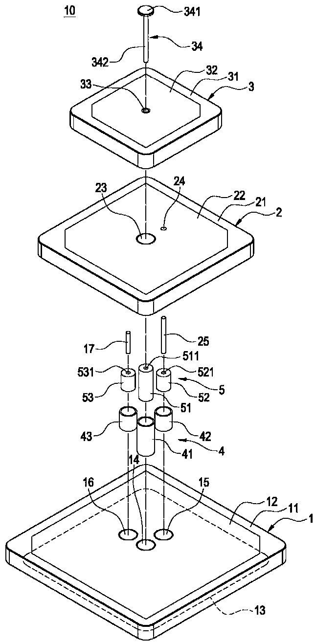
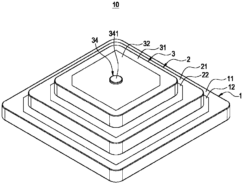
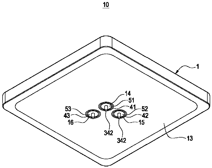
[0023] see Figures 1 to 4 As shown, it is a schematic view of the insulation structure line decomposition, combination bottom view and bottom surface of the ceramic antenna feeding hole of the present invention. As shown in the figure: the ceramic antenna feeding hole insulation structure of the present invention includes: a first antenna 1 , a second antenna 2 , a third antenna 3 , a conductive layer group 4 and a dielectric layer group 5 . Wherein, the first antenna 1, the second antenna 2 and the third antenna 3 are stacked into a three-stacked antenna 10 in an approximate cone shape, and the conductive layer group 4 and the dielectric layer group 5 are arranged on the first antenna 1 and the signal feed-in path of the second antenna 2, the signal feed-in path can achieve impedance matching such as the 50 ohm characteristic of a copper cabl...


PUM


Abstract

The invention discloses a ceramic antenna feed hole insulation structure. The structure comprises a first antenna, a second antenna, a third antenna, a conductive layer group and a first dielectric layer. The first antenna, the second antenna and the third antenna are stacked, then a first conductive layer, a second conductive layer and a third conductive layer of the conductive layer group and afirst dielectric layer, a second dielectric layer and a third dielectric layer of the dielectric layer group are configured in a third through hole, a second through hole and a first through hole of the first antenna and the fourth through hole of the second antenna to allow feed paths of the first feed module of the first antenna, the second feed module of the second antenna and the third feed module of the third antenna to reach impedance characteristics of 50 ohms as a copper-axis cable, the antennas are not mismatched, and the original receiving efficiency of the antennas is ensured.

Description

technical field [0001] The invention relates to an antenna, in particular to a ceramic antenna feed-in hole insulation structure whose feed-in path has the characteristics of a copper-axis cable. Background technique [0002] The wireless communication systems currently used on the market include at least: Global Navigation Satellite System (GNSS), Dedicated Short-Range Communication System (DSRC), Satellite Digital Audio Radio Service System (SDARS), Long Term Evolution Technology System (LTE), wireless network system (WLAN / BT), etc. And the global navigation satellite system includes global, regional and enhanced, such as Global Positioning System (Global Positioning System, GPS), GLONASS (GLONASS) is the global satellite navigation system (GLOBAL NAVIGATION SATELLITE SYSTEM) in Russian The abbreviation of Galileo Positioning System (Galileo), Beidou Satellite Navigation System, and related augmentation systems, such as WAAS (Wide Area Augmentation System), EGNOS (Europea...

Claims


Application Information

Patent Timeline
Patent Type & Authority Applications(China)
IPC IPC(8): H01Q1/38H01Q1/48H01Q1/50
CPCH01Q1/38H01Q1/48H01Q1/50
Inventor 林若南杨才毅
Owner TAOGLAS GROUP HLDG LTD
Why Eureka
Try Eureka