Copper plating method for ceramic substrate

A ceramic substrate and copper plating technology, applied in the electrolytic process, electrolytic components, etc., can solve the problems of poor copper plating thickness uniformity, uneven distribution of power lines, affecting the service life of packaging and finished products, etc., to improve cleanliness, good copper The effect of coating adhesion

Active Publication Date: 2019-08-27
翔声科技(厦门)有限公司
View PDF4 Cites 5 Cited by
  • Summary
  • Abstract
  • Description
  • Claims
  • Application Information

AI Technical Summary

Problems solved by technology

[0004] However, the inventors of the present application have found that during the copper plating process, copper ions move towards the cathode under the action of an electric field, but due to the uneven dist

Method used


Image

  • Copper plating method for ceramic substrate
  • Copper plating method for ceramic substrate
  • Copper plating method for ceramic substrate

Examples


Embodiment 1

[0092] The copper plating method of a kind of ceramic substrate that present embodiment provides, comprises the following steps:

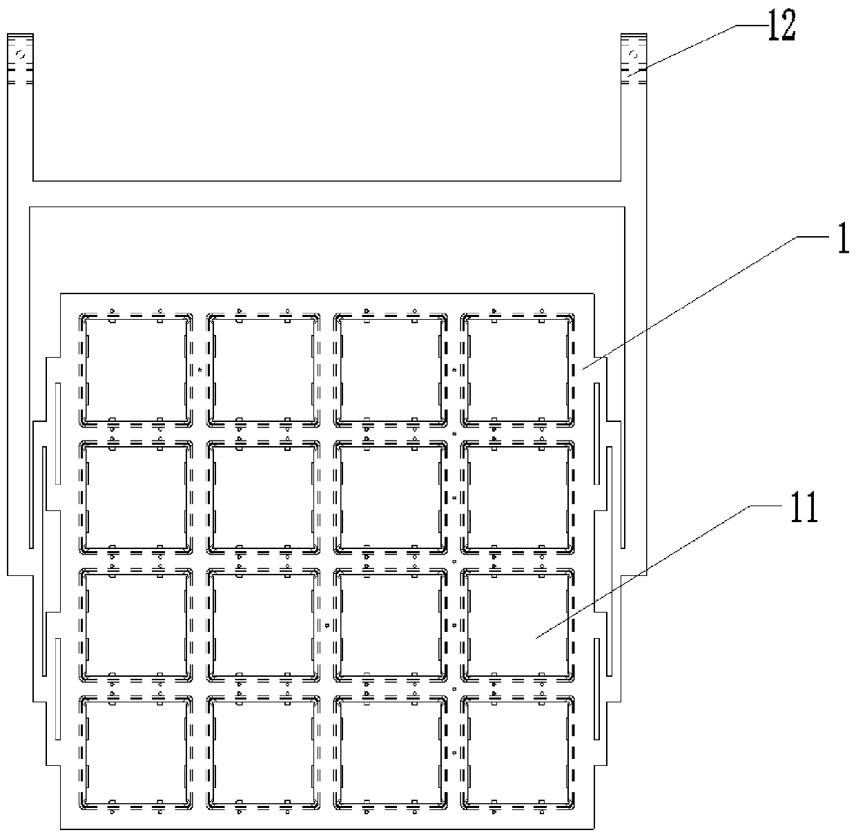
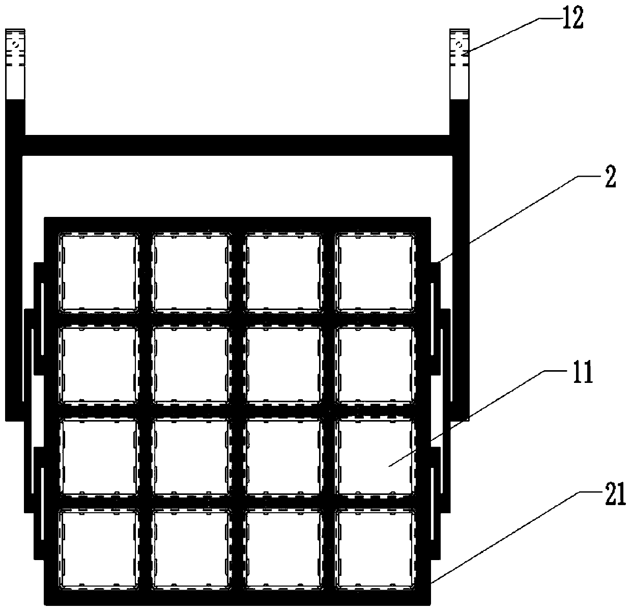
[0093] (1) Mount the ceramic substrate 3 on the mounting hole 11 of the first hanger 1 .

[0094] (2) Carry out surface pretreatment to the first hanger 1 and the ceramic substrate 3; Wherein, the surface pretreatment step is carried out sequentially according to the following steps:

[0095] Degreasing: Soak in surfactant for 90s;

[0096] Pickling: Soak in 4% H by volume fraction 2 60s in SO;

[0097] Double washing: Soak in two water-filled washing tanks for 60 seconds each;

[0098] Hot water washing: Soak in hot water at 60°C for 60s.

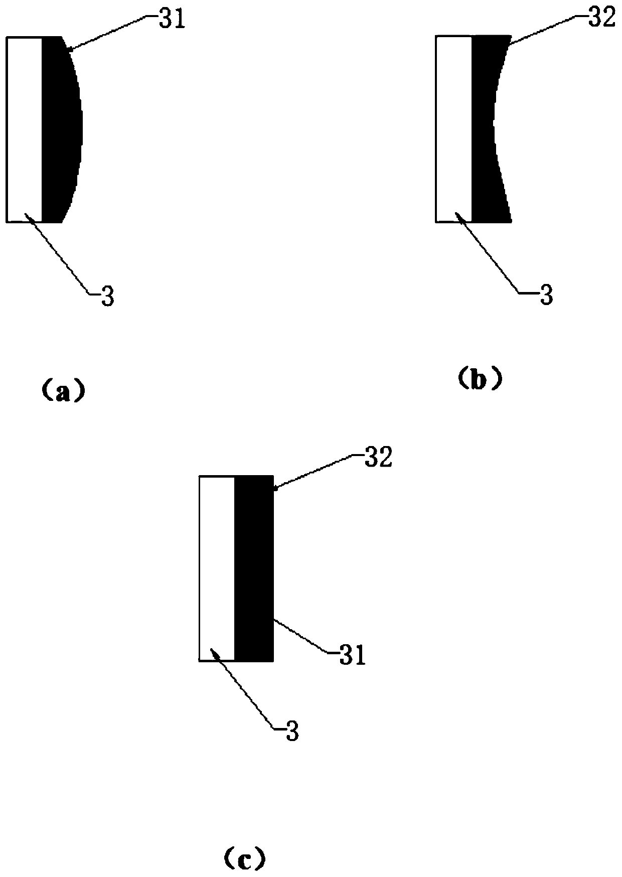
[0099] (3) Copper electroplating for the first time: the first hanger 1 is suspended on the cathode rod of the copper plating tank 4, and the phosphor copper ball is selected as the anode 5; the ceramic substrate 3 is completely immersed in the electroplating solution 6 for the first electroplating of coppe...

Embodiment 2

[0110] The copper plating method of a kind of ceramic substrate that present embodiment provides, and the difference of embodiment 1 is:

[0111] In step (7) second electroplating copper, the ratio of the thickness of the first copper layer 31 and the thickness of the second copper layer 32 is 1.8:1, the thickness of the first copper layer 31 and the thickness of the second copper layer 32 form The copper plating thickness is 70 μm.

Embodiment 3

[0113] The copper plating method of a kind of ceramic substrate that present embodiment provides, and the difference of embodiment 1 is:

[0114] In step (7) second electroplating copper, the ratio of the thickness of the first copper layer 31 and the thickness of the second copper layer 32 is 2.2:1, the thickness of the first copper layer 31 and the thickness of the second copper layer 32 form The copper plating thickness is 80 μm.


PUM


Abstract

The invention provides a copper plating method for a ceramic substrate, and relates to the technical field of electrical copper plating. The method comprises the following steps of: S1, installing theceramic substrate on an installation hole of a first rack, wherein the first rack is made of a conductive material; S2, surface pretreatment; S3, electroplating copper firstly, obtaining an initial plating part; S4, cleaning; S5, transferring the initial plating part to a second rack from the first rack, wherein the second rack is formed by uniformly coating insulation materials on the surface apart from the contact part of the installation hole and a cathode rod; S6, surface pretreatment; S7, electroplating copper secondly, and obtaining a copper plated ceramic substrate; and S8, cleaning. The copper plating layer formed on the ceramic substrate by the above copper plating method has good uniformity, which is favorable for subsequent packaging operations and prolongs the service life ofa finished product.

Description

technical field [0001] The invention relates to the technical field of electroless copper plating, and in particular to a copper plating method for a ceramic substrate. Background technique [0002] Ceramic substrate has excellent thermal conductivity, reliable electrical insulation, low dielectric constant and dielectric loss, and is an ideal heat dissipation packaging material for a new generation of large-scale integrated circuits, semiconductor module circuits and high-power devices. It can be used in high-power power semiconductor modules, semiconductor refrigerators, electronic heaters, power control circuits, automotive electronics, solar panel components, lasers and other fields. The surface of the ceramic substrate often needs to be copper-plated. [0003] The general ceramic substrate copper plating process is: install the ceramic substrate in the hanger, then put the hanger into the copper plating tank filled with electroplating solution, the ceramic substrate to...

Claims


Application Information

Patent Timeline
IPC IPC(8): C25D3/38C25D5/10C25D17/08C25D5/54
CPCC25D3/38C25D5/10C25D5/54C25D17/08
Inventor 曾国书王建国郝涛黄国原夏后雨曹亮李宗超
Owner 翔声科技(厦门)有限公司
Why Eureka
Try Eureka