Semiconductor laser array packaging structure

A technology of laser array and packaging structure, applied in the field of optical communication, to achieve the effect of simple arrangement, large-scale production and clear structure

Active Publication Date: 2019-08-30
宁波东立创芯光电科技有限公司
View PDF18 Cites 0 Cited by
  • Summary
  • Abstract
  • Description
  • Claims
  • Application Information

AI Technical Summary

Problems solved by technology

Therefore, it is impossible to package according to a single EML packaging method, and a new packaging method is needed to solve the packaging problem of array chips

Method used


Image

  • Semiconductor laser array packaging structure
  • Semiconductor laser array packaging structure
  • Semiconductor laser array packaging structure

Examples


Embodiment 1

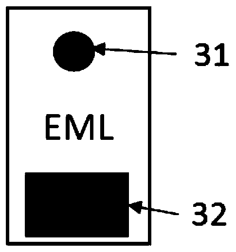
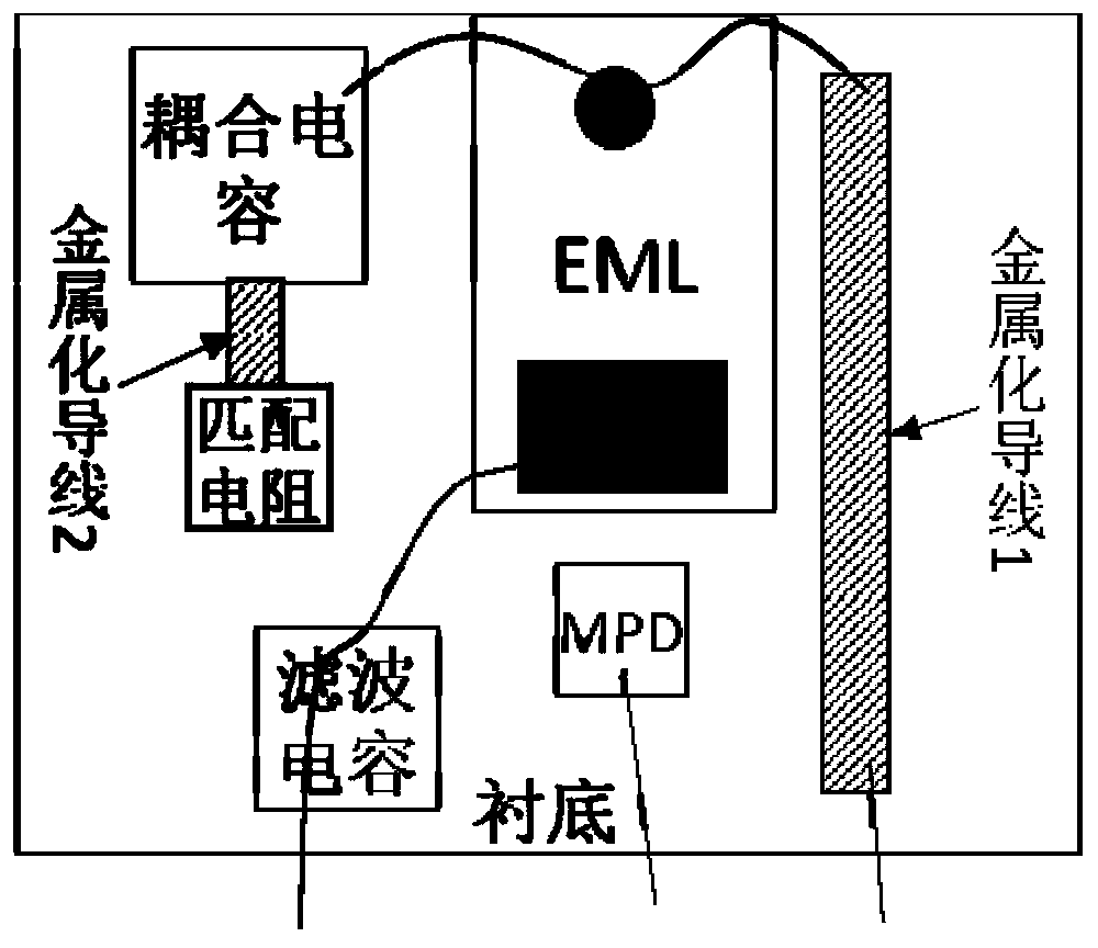
[0043] In addition to the EML array, the materials required for packaging also need a substrate, four filter capacitors, four coupling capacitors, four MPDs and four matching resistors. image 3It is the front structure of the EML array package in this embodiment. The plane where the substrate is located is defined as the xy plane. EML1, EML2, EML3, and EML4 are arranged in sequence along the x direction of the substrate and mounted on the front of the substrate with the back facing up to form an EML unit. ; The filter capacitor 1, the filter capacitor 2, the filter capacitor 3 and the filter capacitor 4 are arranged along the x direction of the substrate and mounted on the front side of the substrate to form a filter capacitor unit; MPD1, MPD2, MPD3 and MPD4 are also sequentially arranged along the substrate The x-direction of the bottom is arranged and mounted on the front of the substrate to form an MPD unit; EML, MPD and filter capacitors correspond one by one, and the EML ...

Embodiment 2

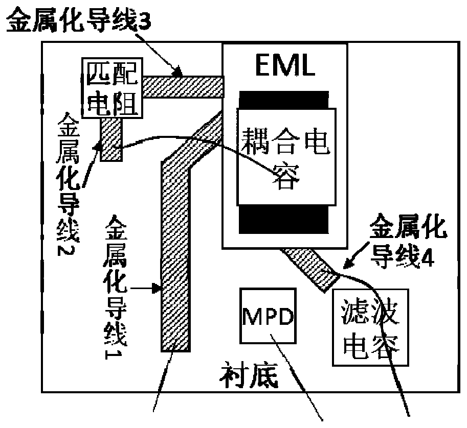
[0048] The difference from Embodiment 1 is that the arrangement of matching resistors and coupling capacitors on the back of the substrate is different. In this embodiment, as Figure 4b ,

[0049] Coupling capacitor 1, coupling capacitor 2, coupling capacitor 3, and coupling capacitor 4 are sequentially arranged along the x direction of the substrate and mounted on the back of the substrate. Matching resistor 1, matching resistor 2, matching resistor 3, and matching resistor 4 are also sequentially arranged along the The x direction of the substrate is arranged and attached to the back of the substrate; eight metallized wires are arranged along the y direction of the substrate (in other embodiments, part of the y direction and part of the x direction can be arranged); The metallized vias are respectively the first metallized via 21, the second metallized via 22, the third metallized via 23 and the fourth metallized via 24. The first metallized via hole 21, the second metalli...

Embodiment 3

[0051] The difference between this embodiment and embodiment one or embodiment two is that, as Figure 4c As shown, the front side of the substrate in this embodiment does not include a filter capacitor, and the pads in the gain region are connected to the outside of the substrate through a metallized wire and a gold wire in turn; the filter capacitor can be located on other substrates to achieve noise filtering.


PUM


Abstract

The invention belongs to the technical field of optical communication, relates to a semiconductor laser array packaging structure and solves a packaging problem of semiconductor laser array chips. N laser chips are all mounted with the back side facing up to a front side of a substrate, n MPDs are mounted on the front side of the substrate, n coupling capacitors and n matching resistors are mounted on a back side of the substrate, an EA pad and a gain pad of each laser chip are sequentially connected with the outside of the substrate through a metallized wire and a gold wire respectively, then MPDs are connected with the outside of the substrate through gold wires, each metallized through hole is connected with the EA pad of one laser chip, each metallized through hole is connected with one end of each coupling capacitor through a metalized wire, and the other ends of the coupling capacitors are respectively connected with the matching resistors through metallized wires. The packagingstructure is advantaged in that the packaging structure can be applied to any external modulated laser array optical devices.

Description

technical field [0001] The invention belongs to the technical field of optical communication, and relates to a semiconductor laser array packaging structure, which can be used for reference in any externally modulated laser (EML: External Modulated Laser) array optical device. Background technique [0002] EML is a semiconductor laser, and the structure of a single EML is as figure 1 As shown, it includes a gain area and a saturable absorption area (EA: ElectroAbsorption), and each area has a pad for the input of electrical signals. The EML needs to go through a packaging process before electrical signals can be introduced into the EML. The basic structure of a single EML package is as follows Figure 2a and Figure 2b As shown, in addition to EML, the materials required for packaging also need a substrate, a filter capacitor, a coupling capacitor, a monitor photodiode (MPD: MonitorPhotoDiode) and a matching resistor. Figure 2a It is a typical packaging structure with E...

Claims


Application Information

Patent Timeline
Patent Type & Authority Applications(China)
IPC IPC(8): H01S5/022H01S5/026H01S5/40
CPCH01S5/0261H01S5/0264H01S5/4025H01S5/02345H01S5/0237
Inventor 徐之光程东马云振
Owner 宁波东立创芯光电科技有限公司
Why Eureka
Try Eureka