Supercharge Your Innovation With Domain-Expert AI Agents!

A kind of three-dimensional circuit board integrated preparation method and three-dimensional circuit board

A circuit board, three-dimensional technology, applied in three-dimensional rigid printed circuit boards, printed circuit manufacturing, printed circuits, etc., can solve the problems of large copper and chemical materials consumption, environmental pollution, and many processes

Active Publication Date: 2020-12-18
北京大华博科智能科技有限公司
View PDF3 Cites 0 Cited by
  • Summary
  • Abstract
  • Description
  • Claims
  • Application Information

AI Technical Summary

Problems solved by technology

[0003] Traditional integrated circuit chip processing or common circuit board manufacturing technologies in various electronic devices are all subtractive manufacturing technologies, that is, removing unnecessary materials by plasma etching or acid corrosion to form a graphic structure of functional materials. The process is complicated, there are many procedures, and it consumes a lot of energy, copper and chemical materials, and the waste water, waste liquid, waste residue and so on also cause serious pollution to the environment.

Method used


Image

  • A kind of three-dimensional circuit board integrated preparation method and three-dimensional circuit board
  • A kind of three-dimensional circuit board integrated preparation method and three-dimensional circuit board
  • A kind of three-dimensional circuit board integrated preparation method and three-dimensional circuit board

Examples


Embodiment 1

[0049] This embodiment provides an integrated preparation method for a three-dimensional circuit board, which is applied to a three-dimensional printing device equipped with an insulating ink extrusion head and a conductive ink extrusion head; the method includes the following steps:

[0050] (1) Constructing a three-dimensional model file according to the three-dimensional structure of the three-dimensional circuit board to be prepared; layering and slicing the three-dimensional model file to generate a printing program;

[0051] (2) Under the environment of UV light radiation, according to the printing program, use the insulating ink extrusion head to print UV insulating ink on the surface of the printing platform, and obtain a supporting substrate after curing;

[0052] (3) Under the environment of UV light radiation, according to the printing program, use the insulating ink extrusion head to print UV insulating ink on the surface of the supporting substrate, and obtain an ins...

Embodiment 2

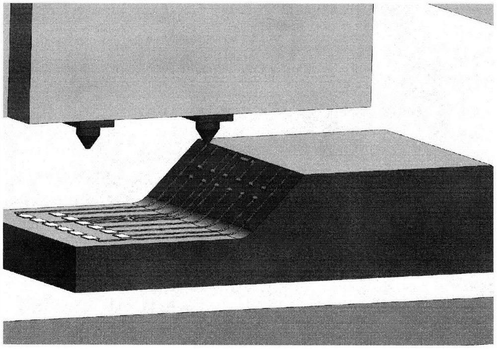
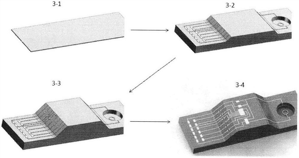
[0085] refer to image 3 , the present embodiment provides a fluid printing method based on dual extrusion heads alternately and cooperatively in a closed UV light radiation environment, so as to realize the integrated fabrication of three-dimensional circuits. Specifically include the following steps.

[0086] (1) According to image 3 Create a 3D model file for the raised circuit board shown in 3-4. Based on the graphic digital slicing technology, the 3D circuit is layered and sliced, the optimized digital slicing algorithm and the nozzle walking path are selected, and the printing program is generated.

[0087] (2) Printing support substrate: Based on the fluid extrusion printing method, UV-curable insulating ink is printed on the surface of the printing platform, and the printed UV insulating ink is gradually cured and formed as a support substrate in a UV light radiation environment. The obtained support substrate is as image 3 as shown in 3-1.

[0088] (3) Print the...

Embodiment 3

[0092] refer to image 3 , the present embodiment provides a fluid printing method based on dual extrusion heads alternately and cooperatively in a closed UV light radiation environment, so as to realize the integrated production of spatial curved surface circuits. Specifically include the following steps.

[0093] (1) According to Figure 4 Create a three-dimensional model file for the space surface circuit shown in 4-4. Based on the graphic digital slicing technology, perform layered slicing processing on the space surface circuit, select the optimized digital slicing algorithm and nozzle walking path, and generate a printing program.

[0094] (2) Printing support substrate: Based on the fluid extrusion printing method, UV-curable insulating ink is printed on the surface of the printing platform, and the printed UV insulating ink is gradually cured and formed as a support substrate in a UV light radiation environment. supporting substrate such as Figure 4 shown in 4-1. ...


PUM

PropertyMeasurementUnit
wavelengthaaaaaaaaaa

Abstract

The embodiment of the invention relates to an integrated preparation method of a three-dimensional circuit board and a three-dimensional circuit board. The method comprises the following steps of: (1)constructing a three-dimensional model file according to the three-dimensional structure of a three-dimensional circuit board to be prepared, and performing layered slicing on the three-dimensional model file to generate a printing program; (2) printing UV insulating ink on the surface of a printing platform by using the insulating ink extrusion head according to the printing program in the environment of UV light radiation, and performing curing to obtain a supporting substrate; (3) printing UV insulating ink on the surface of the supporting substrate by using the insulating ink extrusion head according to the printing program in the environment of UV light radiation, and performing curing to obtain an insulating layer; and (4) and printing UV conductive ink on the area outside the insulating layer on the surface of the supporting substrate by using the conductive ink extrusion head according to the printing program under the environment of UV light radiation, and performing wiring.

Description

technical field [0001] The embodiments of the present invention relate to the technical field of circuit boards, and in particular to an integrated preparation method for a three-dimensional circuit board and a three-dimensional circuit board. Background technique [0002] The circuit board is an important electronic component, a support for electronic components, and a carrier for electrical connections of electronic components. Almost all electronic devices are inseparable from circuit boards, from electronic watches, general-purpose computers, televisions, to supercomputers, communication electronic equipment, military weapon systems, etc., as long as there are electronic components such as integrated circuits, they are electrically interconnected All circuit boards are used. [0003] Traditional integrated circuit chip processing or common circuit board manufacturing technologies in various electronic devices are all subtractive manufacturing technologies, that is, remo...

Claims


Application Information

Patent Timeline
Patent Type & Authority Patents(China)
IPC IPC(8): H05K3/00H05K3/12H05K1/02
CPCH05K1/0284H05K3/0011H05K3/1241H05K2203/0545
Inventor 不公告发明人
Owner 北京大华博科智能科技有限公司
Features
  • R&D
  • Intellectual Property
  • Life Sciences
  • Materials
  • Tech Scout
  • Unparalleled Data Quality
  • Higher Quality Content
  • 60% Fewer Hallucinations
Learn More