Supercharge Your Innovation With Domain-Expert AI Agents!

A packaging method for wafer-level infrared detection chips

A technology of infrared detection and packaging method, which is applied in the direction of radiation control devices, semiconductor devices, electrical components, etc. It can solve the problems of too small size of solder sheet, inability to align, deformation, etc., and achieve the effect of high yield rate and high precision of finished products

Active Publication Date: 2020-12-15
JIANGSU PROSPER SEMICON INC
View PDF4 Cites 0 Cited by
  • Summary
  • Abstract
  • Description
  • Claims
  • Application Information

AI Technical Summary

Problems solved by technology

Since infrared detectors have been developed to wafer-level packaging, the size is getting smaller and smaller, and the size of the solder sheet is also reduced. This has caused a large increase in the deformation of the solder sheet production, and the process of picking and placing materials at the packaging end also has this deformation problem.
When the size needs to be further reduced, the size of the solder sheet is too small, the manufacturer is difficult to manufacture, and it is difficult for personnel to pick and place during production, and the solder is easily deformed and cannot be aligned.

Method used


Image

  • A packaging method for wafer-level infrared detection chips
  • A packaging method for wafer-level infrared detection chips
  • A packaging method for wafer-level infrared detection chips

Examples


Embodiment Construction

[0024] The present invention will be further described below in conjunction with the accompanying drawings and specific embodiments, so that those skilled in the art can better understand the present invention and implement it, but the examples given are not intended to limit the present invention.

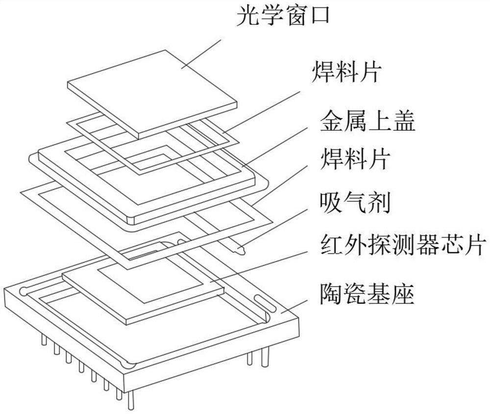
[0025] refer to Figure 2-Figure 3 As shown, the present invention discloses a packaging method for a wafer-level infrared detection chip, based on a vacuum reflow soldering machine, the vacuum reflow soldering machine includes an upper cavity and a lower cavity, and the gap between the upper cavity and the lower cavity is Setting a shutter includes the following steps:

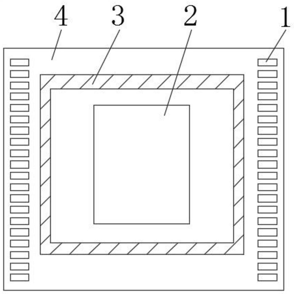
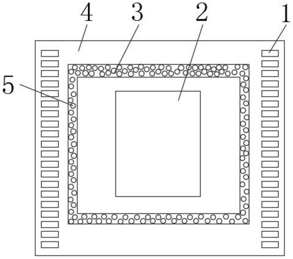
[0026] Step 1, the infrared detection chip 4 includes a photosensitive area 2, a metallized area 3 is arranged around the photosensitive area 2, and a metal layer is arranged on the metallized area 3. Two rows of gold-plated pads 1 are arranged on the infrared detection chip 4, and the metallization area 3 is lo...


PUM


Abstract

Disclosed in the present invention is a packaging method for a wafer-level infrared detection chip, comprising the following steps: step I, providing a metal layer in a metallized region of an infrared detection chip; step II, placing a first material in an upper cavity, the first material comprising the infrared detection chip having the metal layer, and then heating the upper cavity to a first temperature and maintaining the temperature; step III, placing a second material in a lower cavity, the second material comprising an optical window and a getter, and then sequentially performing degassing treatment and activation treatment on the second material in the lower cavity; step IV, opening a shielding plate, heating a vacuum reflow welding machine to a welding temperature, and maintaining the temperature, the welding temperature being a melting point of the metal layer, the metal layer being molten at the welding temperature, and the infrared detection chip and the optical window being combined together by the molten metal layer; and step V, stopping heating the vacuum reflow welding machine, naturally cooling to room temperature, and taking out a finished product. The method is applicable to packaging of a wafer-level infrared detection chip, high in precision, and high in yield of the finished product.

Description

technical field [0001] The invention relates to the field of infrared chip packaging, in particular to a method for packaging a wafer-level infrared detection chip. Background technique [0002] At present, the infrared image sensor includes an infrared detection chip, and a commonly used packaging method for the infrared detection chip is ceramic packaging. like figure 1 As shown, it is a schematic diagram of firing in the traditional infrared packaging technology. The ceramic package includes a ceramic base, a metal upper cover and an optical window, and the three form a vacuum cavity; an infrared detector chip is installed on the ceramic base, and an absorbing Air agent, coated with infrared green light film on the optical window, during packaging, the optical window / metal upper cover / ceramic base is heated at high temperature in a vacuum environment, and the getter is activated, and then the optical window / metal upper cover / ceramic base , welded together again with a s...

Claims


Application Information

Patent Timeline
Patent Type & Authority Patents(China)
IPC IPC(8): H01L27/146
CPCH01L27/14618H01L27/14634H01L27/14636H01L27/1469
Inventor 林明芳陈俊宇郭信良
Owner JIANGSU PROSPER SEMICON INC
Features
  • R&D
  • Intellectual Property
  • Life Sciences
  • Materials
  • Tech Scout
  • Unparalleled Data Quality
  • Higher Quality Content
  • 60% Fewer Hallucinations
Learn More