Automatic chip mounting mechanism

An automatic patch and patch technology, applied in electrical components, printed circuit manufacturing, electrical components, etc., can solve the problems of product quality, dislocation of tin, and high cost

Pending Publication Date: 2019-08-30
苏州睿立汇自动化科技有限公司
View PDF0 Cites 5 Cited by
  • Summary
  • Abstract
  • Description
  • Claims
  • Application Information

AI Technical Summary

Problems solved by technology

[0002] In the process of circuit board manufacturing, it is necessary to perform tin spotting and pasting chip operations inside. The traditional tin spotting and chip pasting operations are divided into multiple stations. The products must be positioned one by one and tinned one by one. If the positioning process products Movement, resulting in dislocation of tin points, resulting in product quality problems; in the placement operation, it is necessary to first rotate the angle of the chip, and then align it with the angle of the product to attach it. The robot directly picks up and rotates the operation, which is easy to make the positioning of the product deviate, and The method of clamping and positioning one by one has low work efficiency, and the linkage equipment involved in the manipulator is more complicated and the cost is high

Method used


Image

  • Automatic chip mounting mechanism
  • Automatic chip mounting mechanism
  • Automatic chip mounting mechanism

Examples


Embodiment

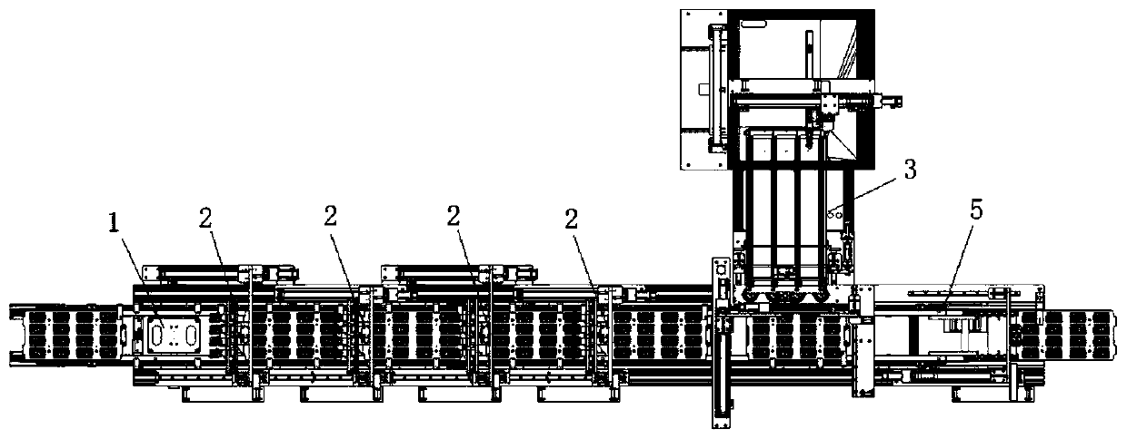
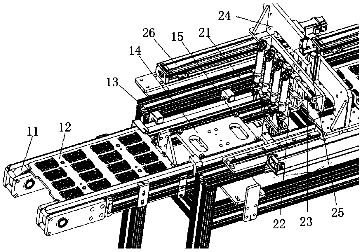
[0032] refer to Figure 1-9 As shown, the present embodiment is an automatic placement mechanism, including a feeding device 1 , several tin spotting devices 2 cooperating with the feeding device 1 , a placement device 3 , and a feeding device 5 .

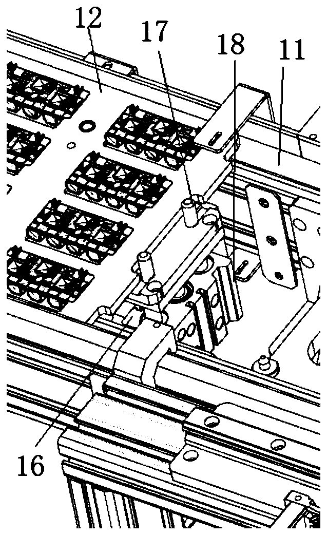
[0033] The feeding device 1 includes a conveyor belt 11 , a number of ejector components arranged at intervals below the conveyor belt 11 , and stopper assemblies arranged at both ends of each ejector assembly.

[0034] The inner side of the conveyor belt 11 carries and transports a number of product carriers 12, and the two sides of the conveyor belt 11 are symmetrically provided with a number of locking blocks 13, and the bottom of the locking blocks 13 is placed above the side of the product carrier 12 for limiting product loading. The position height of tool 12 in conveyor belt 11.

[0035] The ejector assembly includes an extended jacking product carrier 12 located below the conveyor belt 11 to separate it from the top plate ...


PUM


Abstract

The present invention discloses an automatic chip mounting mechanism. The mechanism comprises a feeding device, a plurality of tin-soldering devices matched with the feeding device, and a chip mounting device. A material ejection component comprises a top plate arranged at the lower portion of a conveyer belt and used for extending and top connection with a product carrier to break away the product carrier from the conveyer belt, a material blocking component comprises a blocking post extended to the side of the product carrier to limit the movement of the product carrier along the conveyer belt, each tin-soldering device comprises a plurality of tin-soldering needle tips horizontally and vertically moving arranged at the upper portion of the product carrier, the chip mounting device comprises a material taking component configured to convey a chip, a rotation component configured to rotate and locate the chip and an attaching component, the material taking component comprises a lifting material taking sucking disc, the rotation component comprises a rotationally arranged rotation platform, the material taking sucking disc sucks the chip to be located at the rotation platform, andthe attaching component comprises an attaching sucking disc configured to absorb the chip on the rotation platform in a lifting movement mode and transmit the chip onto the product carrier in the conveyer belt. The automatic chip mounting mechanism achieves automatic product feeding and chip mounting, and improves the processing efficiency.

Description

technical field [0001] The invention belongs to the technical field of circuit board manufacturing, and in particular relates to an automatic patch mechanism. Background technique [0002] In the process of circuit board manufacturing, it is necessary to perform tin spotting and pasting chip operations inside. The traditional tin spotting and chip pasting operations are divided into multiple stations. The products must be positioned one by one and tinned one by one. If the positioning process products Movement, resulting in dislocation of tin points, resulting in product quality problems; in the placement operation, it is necessary to first rotate the angle of the chip, and then align it with the angle of the product to attach it. The robot directly picks up and rotates the operation, which is easy to make the positioning of the product deviate, and The way of clamping and positioning one by one has low work efficiency, and the linkage equipment involved in the manipulator i...

Claims


Application Information

Patent Timeline
Patent Type & Authority Applications(China)
IPC IPC(8): H05K3/30H05K13/04H05K3/34
CPCH05K3/303H05K3/341H05K13/0408H05K13/0417
Inventor 裴昊
Owner 苏州睿立汇自动化科技有限公司
Why Eureka
Try Eureka