Processing device for third-generation semiconductor material

A processing device and semiconductor technology, which is applied in semiconductor/solid-state device manufacturing, electrical components, circuits, etc., can solve the problems of lower production efficiency, low degree of integration, slow conversion speed, etc., and achieve high processing efficiency and high degree of integration , improve the effect of the effect

Active Publication Date: 2019-09-06
江苏守航实业有限公司
View PDF5 Cites 1 Cited by
  • Summary
  • Abstract
  • Description
  • Claims
  • Application Information

AI Technical Summary

Problems solved by technology

[0003] At present, the third-generation semiconductors need to be corroded and cleaned during the processing process. Through the chemical reaction between the chemical solution and the corroded object, the atoms on the surface are removed. Generally, it needs to go through steps such as corrosion cleaning, washing, and drying. The low degree of integration and the slow conversion speed between each step reduce the production efficiency

Method used


Image

  • Processing device for third-generation semiconductor material
  • Processing device for third-generation semiconductor material
  • Processing device for third-generation semiconductor material

Examples


Embodiment Construction

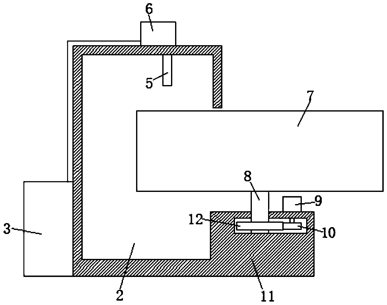
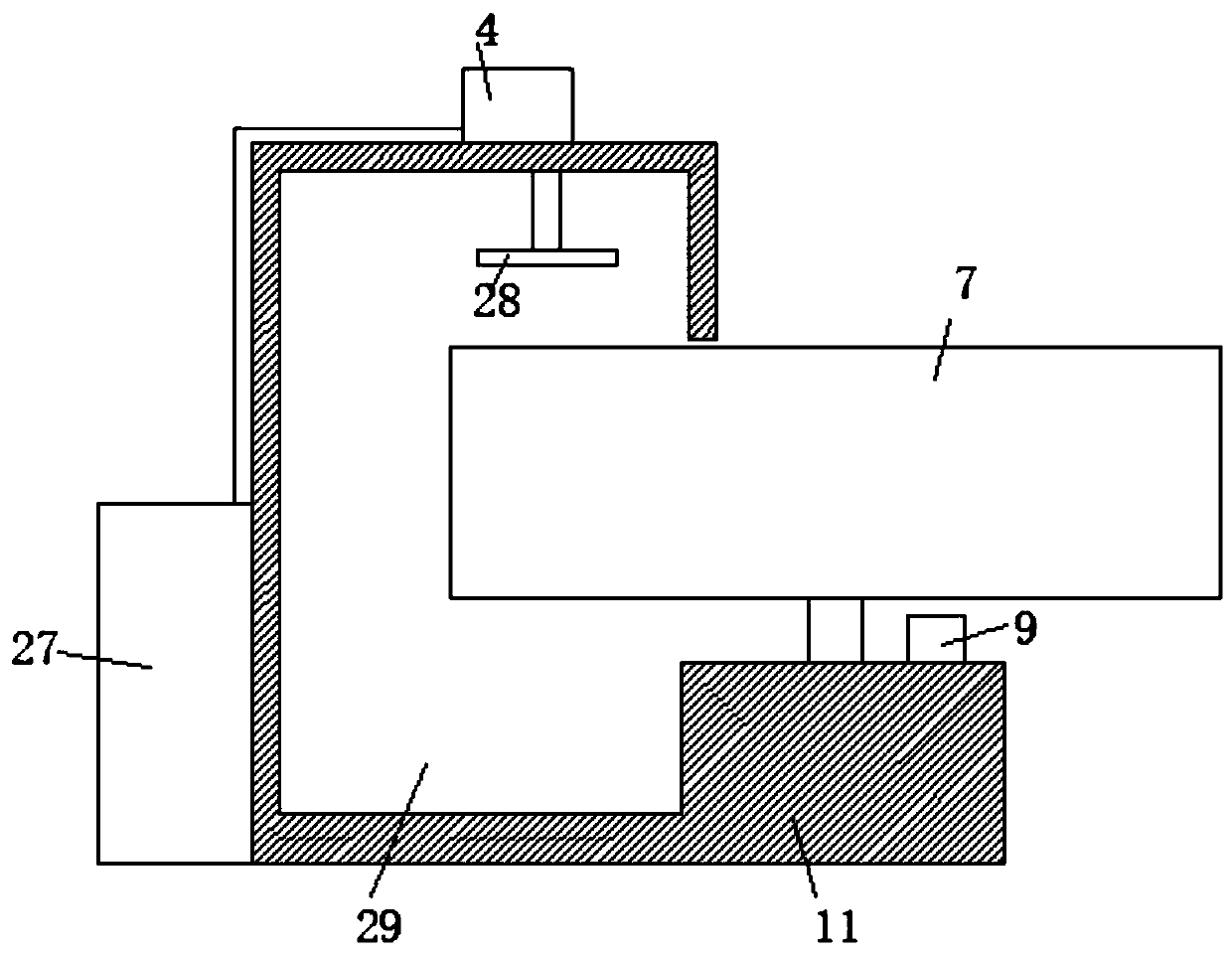
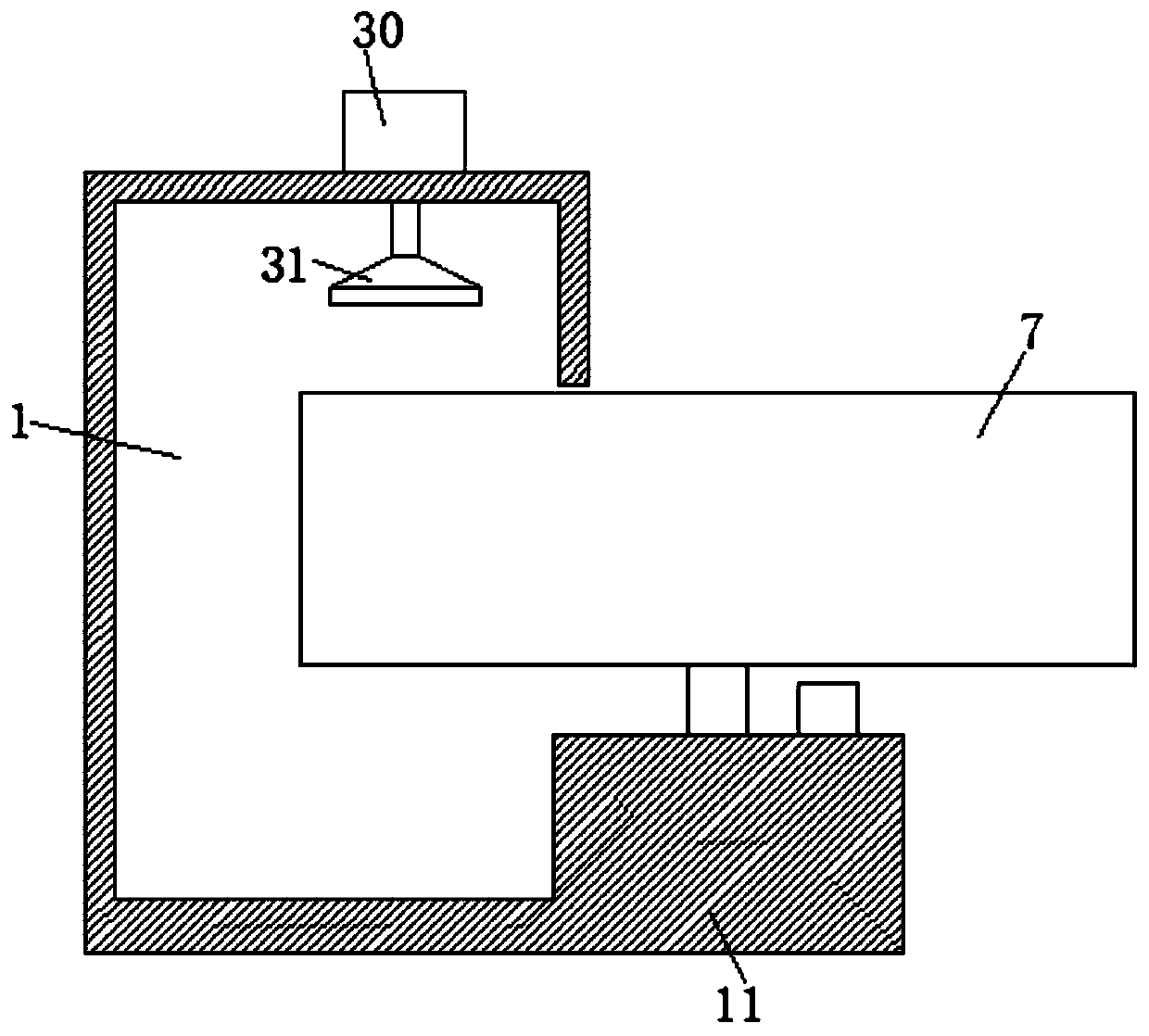
[0024] In order to make the above objects, features and advantages of the present invention more comprehensible, specific implementations of the present invention will be described in detail below in conjunction with the accompanying drawings. In the following description, numerous specific details are set forth in order to provide a thorough understanding of the present invention. However, the present invention can be implemented in many other ways different from those described here, and those skilled in the art can make similar improvements without departing from the connotation of the present invention, so the present invention is not limited by the specific implementations disclosed below.

[0025] It should be noted that when an element is referred to as being “fixed” to another element, it can be directly on the other element or there can also be an intervening element. When an element is referred to as being "connected to" another element, it can be directly connected ...


PUM


Abstract

The invention relates to the technical field of third-generation semiconductor materials, in particular to a processing device for a third-generation semiconductor material, and aims at solving the problems of low integration degree, low conversion speed and the like in the prior art; a solution is proposed as follows: the processing device comprises a processing table, wherein a corrosion chamber, a cleaning chamber and a drying chamber are arranged in the machining table; a mounting cavity is formed in the bottom of the processing table; a rotating mechanism is arranged in the mounting cavity; a rotating disc connected with the rotating mechanism is arranged on the processing table; the part of the rotating disc extends to the corrosion chamber, the cleaning chamber and the drying chamber; a plurality of placing grooves are formed in the circumferential direction of the upper end of the rotating disc at equal intervals, wherein three of the placing grooves are positioned in the corrosion chamber, the cleaning chamber and the drying chamber respectively; and a corrosion mechanism is arranged on the inner top of the corrosion chamber. The processing device disclosed by the invention has the advantages that the structure is reasonable, the corrosion, cleaning, washing and drying are integrated, the integration degree is high, and the feeding and processing can be continuously carried out.

Description

technical field [0001] The invention relates to the technical field of third-generation semiconductor materials, in particular to a processing device for third-generation semiconductor materials. Background technique [0002] With the continuous expansion of the application field of semiconductor devices, especially in special occasions, semiconductors are required to remain strong in high temperature, strong radiation, high power and other environments. The first and second generation semiconductor materials are powerless, so the third generation of semiconductor materials - wide Bandgap semiconductor materials (bandgap width greater than 2.2ev) have become the focus of attention, mainly including silicon carbide (SiC), gallium nitride (GaN), gallium arsenide (GaAS), zinc oxide (ZnO), diamond, nitride Aluminum (AlN), more mature silicon carbide and gallium nitride are known as the duo of the third-generation semiconductor materials, while the research on zinc oxide, diamond...

Claims


Application Information

Patent Timeline
Patent Type & Authority Applications(China)
IPC IPC(8): H01L21/67
CPCH01L21/67155
Inventor 魏守冲
Owner 江苏守航实业有限公司
Why Eureka
Try Eureka