Array substrate, manufacturing method thereof and liquid crystal display panel

A technology for array substrates and display areas, applied in static indicators, nonlinear optics, instruments, etc., can solve problems such as poor display

Inactive Publication Date: 2019-09-10
HKC CORP LTD +1
View PDF8 Cites 6 Cited by
  • Summary
  • Abstract
  • Description
  • Claims
  • Application Information

AI Technical Summary

Problems solved by technology

[0004] The invention provides an array substrate and its manufacturing method and a liquid crystal display panel to solve the problem of bad display caused by laser cutting

Method used


Image

  • Array substrate, manufacturing method thereof and liquid crystal display panel
  • Array substrate, manufacturing method thereof and liquid crystal display panel
  • Array substrate, manufacturing method thereof and liquid crystal display panel

Examples


Embodiment Construction

[0028]In order to make the above objects, features and advantages of the present invention more comprehensible, specific implementations of the present invention will be described in detail below in conjunction with the accompanying drawings. In the following description, numerous specific details are set forth in order to provide a thorough understanding of the present invention. However, the present invention can be implemented in many other ways different from those described here, and those skilled in the art can make similar improvements without departing from the connotation of the present invention, so the present invention is not limited by the specific implementations disclosed below.

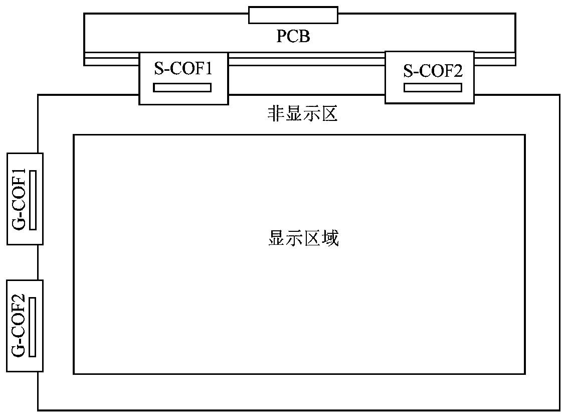
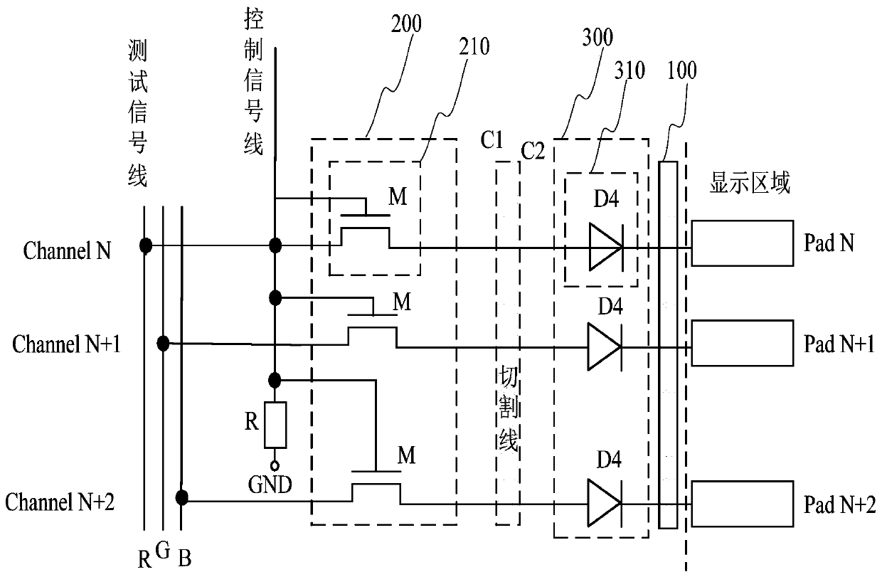
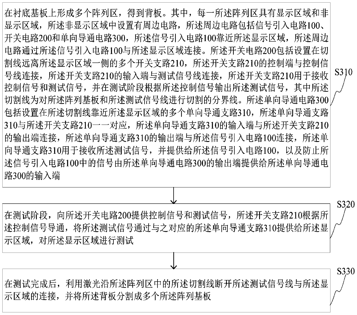
[0029] In view of the above problems, an embodiment of the present invention provides an array substrate. See figure 1 and figure 2 , the array substrate includes a display area and a non-display area, and peripheral circuits are arranged in the non-display area, and the peripheral ...


PUM


Abstract

The invention provides an array substrate, a manufacturing method thereof and a liquid crystal display panel. The array substrate comprises a display area and a non-display area, wherein a peripheralcircuit is arranged in the non-display area and comprises a signal lead-in circuit, a switch circuit and an unidirectional conduction circuit. The switch circuit comprises a plurality of switch branches arranged on one side, far away from the display area, of the cutting line, the control ends of the switch branches are connected with control signal lines, the input ends of the switch branches areconnected with test signal lines and used for outputting test signals according to the control signals in a test stage, and the cutting line is a boundary for cutting the array substrate and the testsignal lines. The unidirectional conducting circuit comprises a plurality of unidirectional conducting branches arranged between the cutting line and the signal leading-in circuit, the unidirectionalconducting branches are in one-to-one correspondence with the switch branches, the unidirectional conducting branches provide received test signals to the signal leading-in circuit, and signals in the signal leading-in circuit are prevented from being provided to the input end of the unidirectional conducting circuit by the output end of the unidirectional conducting circuit.

Description

technical field [0001] The invention relates to the field of display technology, in particular to an array substrate, a manufacturing method thereof, and a liquid crystal display panel. Background technique [0002] The Thin Film Transistor Liquid Crystal Display (TFT-LCD) panel is one of the main products of the current flat panel display, and has become an important display platform in the modern information technology industry and video products. The main driving principle of the TFT-LCD display panel includes: the main board of the system connects data such as pixel signals and control signals and the power supply to the connector on the printed circuit board (Printed Circuit Board, PCB) through the wire, and the data passes through the logic on the PCB board. Board (Timing Controller, TCON) integrated circuit processing, through the PCB board, through the source film drive chip (Source-Chip on Film, S-COF) and gate film drive chip (Gate-Chip on Film, G-COF) and The dis...

Claims


Application Information

Patent Timeline
IPC IPC(8): G02F1/1345G02F1/1362G09G3/00
CPCG02F1/13452G02F1/1362G09G3/006G02F1/136254
Inventor 黄笑宇
Owner HKC CORP LTD
Why Eureka
Try Eureka