Display device

A display device and substrate technology, which is applied in the direction of instruments, nonlinear optics, optics, etc., can solve the problems of light leakage and contrast reduction of display devices, and achieve the effects of increasing contrast, reducing brightness, and reducing light leakage

Active Publication Date: 2019-09-10
KUSN INFOVISION OPTOELECTRONICS
View PDF4 Cites 11 Cited by
  • Summary
  • Abstract
  • Description
  • Claims
  • Application Information

AI Technical Summary

Problems solved by technology

[0005] In order to overcome the disadvantages and deficiencies in the prior art, the purpose of the present invention is to provide a d

Method used


Image

  • Display device
  • Display device
  • Display device

Examples


Embodiment 1

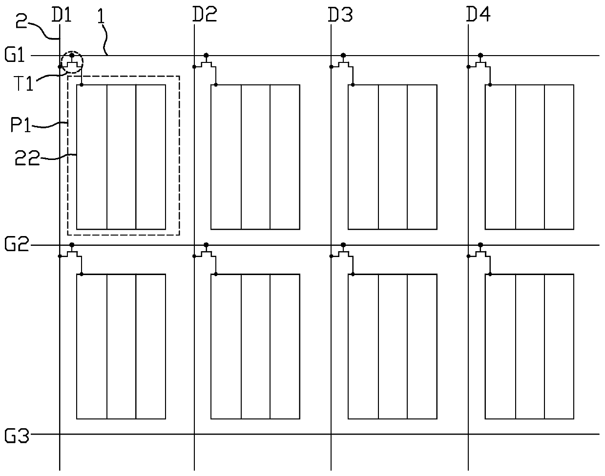
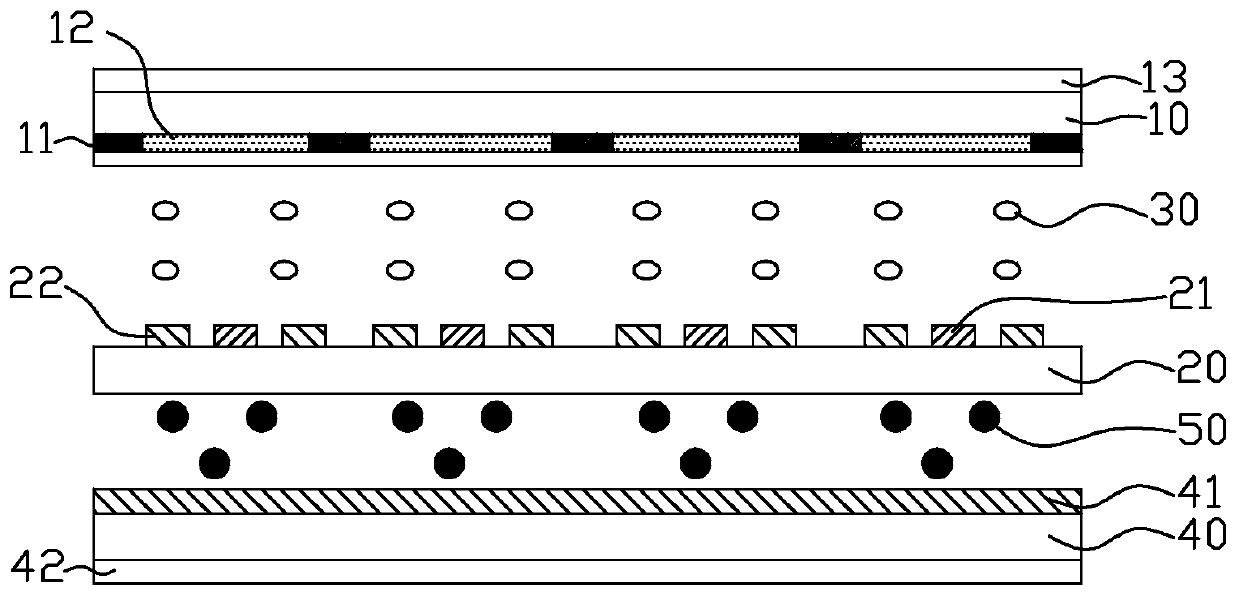
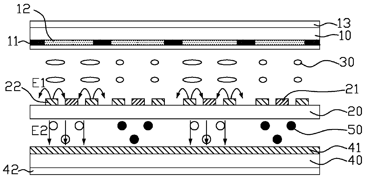
[0031] figure 1 is a schematic plan view of the pixel electrode in Embodiment 1 of the present invention, figure 2 is a schematic cross-sectional structure diagram of the display device in the initial state in Embodiment 1 of the present invention, image 3 It is a schematic diagram of the cross-sectional structure of the display device in the first embodiment of the present invention when it is working, Figure 4 yes image 3 A simulation of light passing through a display device.

[0032] Such as Figure 1 to Figure 4 As shown, the display device provided by Embodiment 1 of the present invention includes a first substrate 10, a second substrate 20 disposed below the first substrate 10, and a liquid crystal layer 30 located between the first substrate 10 and the second substrate 20. The side of the second substrate 20 facing the liquid crystal layer 30 is defined by a plurality of first scanning lines 1 and a plurality of data lines 2 mutually insulated and intersecting ...

Embodiment 2

[0040] Figure 5 is a schematic plan view of the first electrode in Embodiment 2 of the present invention, Figure 6 It is a schematic cross-sectional structure diagram of the display device in the second embodiment of the present invention when it is working. Such as Figure 5 and Figure 6 As shown, the display device provided by Embodiment 2 of the present invention is the same as Embodiment 1 ( figure 1 and image 3 ) are basically the same in structure and working principle, the difference is that in this embodiment, the first electrode 41 is a patterned structure formed by a plurality of first electrode blocks 411 spaced apart from each other, and the third substrate 40 On the side facing the polymer liquid crystal layer 50, a plurality of second scanning lines 3 and a plurality of first common lines 4 are mutually insulated and intersected to define a plurality of second pixel units P2, and the plurality of second pixel units P2 are respectively connected to a plura...

Embodiment 3

[0046] Figure 7 It is a schematic diagram of the cross-sectional structure of the display device in the third embodiment of the present invention when it is working. Such as Figure 7 As shown, the display device provided by Embodiment 3 of the present invention is the same as Embodiment 2 ( Figure 6 ) are basically the same in structure and working principle, the difference is that in this embodiment, the second substrate 20 is provided with a second electrode 61 on the entire surface on the side facing the polymer liquid crystal layer 50 . The second electrode 61 is used to apply a DC voltage signal (for example, 0V), and the first electrode 41 is used to apply an AC voltage signal that fluctuates up and down centered on the DC voltage signal, so that there is a relatively large gap between the first electrode 41 and the second electrode 61. A large voltage difference (for example, 5V) is used to control the switching of the polymer liquid crystal layer 50 between the tr...


PUM


Abstract

The invention discloses a display device, whichcomprises a first substrate and a second substrate arranged under the first substrate. The second substrate is further provided with a common electrode on the side facing the first substrate, each of first pixel units is provided with a pixel electrode and a first thin film transistor, the pixel electrode is electrically connected to a first scan lineand a data line adjacent to the first thin film transistor through the first thin film transistor, a third substrate and a polymer liquid crystal layer located between the second substrate and the third substrate are arranged under the second substrate, the third substrate is provided with a first electrode on the side facing the polymer liquid crystal layer, and the electric field in the polymerliquid crystal layer in a region corresponding to each of the first pixel units is separately controlled so that the polymer liquid crystal layer and the region corresponding to each of the first pixel units are individually switchable between a transparent state and a hazy state; and light leakage of the display device in a dark state can be reduced, and contrast is increased.

Description

technical field [0001] The invention relates to the technical field of liquid crystal display, in particular to a display device. Background technique [0002] A thin film transistor liquid crystal display (Thin Film Transistor-Liquid Crystal Display, TFT-LCD) includes a color filter substrate (Color Filter Substrate, CF Substrate) and a thin film transistor array substrate (Thin Film Transistor Substrate, TFT Substrate). transparent electrodes. A layer of liquid crystal molecules (Liquid Crystal, LC) is sandwiched between the two substrates. The liquid crystal display controls the orientation of the liquid crystal molecules through the electric field, changes the polarization state of the light, and realizes the purpose of display by using the polarizer to realize the penetration and blocking of the light path. [0003] On the other hand, Polymer Dispersed Liquid Crystal (PDLC), as a liquid crystal dimming valve, has been widely concerned and used in recent years. It is ...

Claims


Application Information

Patent Timeline
IPC IPC(8): G02F1/1347G02F1/1343G02F1/1362
CPCG02F1/13476G02F1/134309G02F1/136286
Inventor 王旭宏王小荣沈红福谢爱庆罗雨钟
Owner KUSN INFOVISION OPTOELECTRONICS
Why Eureka
Try Eureka