A pixel matrix driving method and display device
A technology of a pixel matrix and a driving method, applied in the field of a pixel matrix driving method and a display device, can solve the problems of increased manufacturing cost, increased panel power consumption, poor user experience, etc., and achieves the advantages of reducing cost, reducing power consumption and avoiding crosstalk. Effect
- Summary
- Abstract
- Description
- Claims
- Application Information
AI Technical Summary
Problems solved by technology
Method used
Image

Examples
Embodiment 1
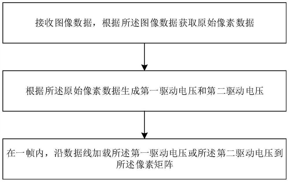
[0050] See figure 2 , figure 2It is a flow chart of a pixel matrix driving method provided by an embodiment of the present invention. The pixel matrix driving method is suitable for current displays with pixel arrays, such as LCD displays, LED displays, OLED displays and the like.
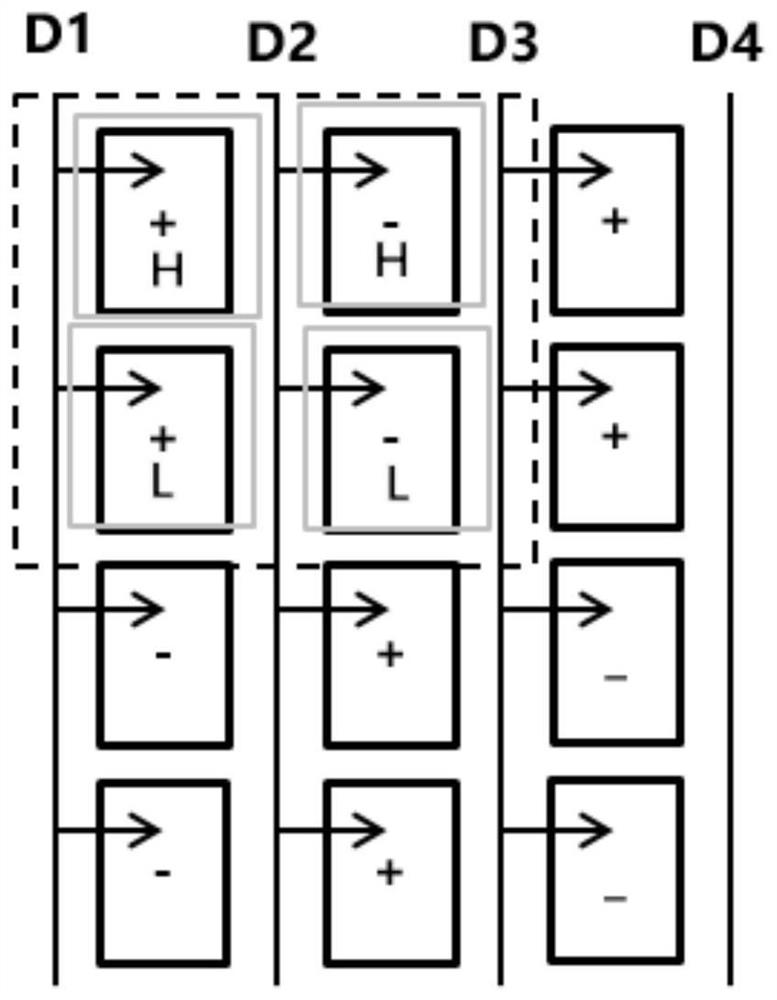
[0051] The pixel matrix includes a plurality of sub-pixels arranged in a matrix, the polarity of the data line is reversed every two columns, the voltage applied along the direction of the data line is switched every N sub-pixels, and every N sub-pixels, Each data line alternately applies a voltage to the subpixels in the Ith column and the I+2th column, wherein the method includes:
[0052] Step 1. Receive image data, and obtain original pixel data according to the image data;
[0053] Step 2, generating a first driving voltage and a second driving voltage according to the original pixel data;
[0054] Step 3. In one frame, apply the first driving voltage or the second driving voltage to the...
Embodiment 2
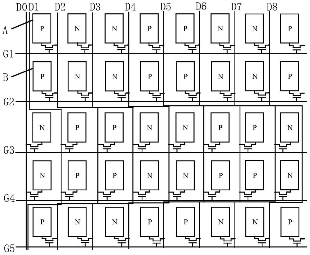
[0082] In a specific implementation manner, corresponding to one of the above solutions, in order to show the solutions of the present invention more clearly, please refer to Figure 5-Figure 6 , Figure 5 , Image 6 is a schematic diagram of a part of the pixel matrix when N=2.
[0083] Among them, D0 data line connects sub-pixels A31, A41, D1 data line connects sub-pixels A32, A42, D2 data line connects sub-pixels A11, A21, A33, A43, A51, D3 data line connects sub-pixels A12, A22, A34, A44, A52, D4 data lines connect sub-pixels A13, A23, A35, A45, A53, D5 data lines connect sub-pixels A14, A24, A36, A46, A54, D6 data lines connect sub-pixels A15, A25, A37, A47, A55, D7 data line connects sub-pixels A16, A26, A38, A48, A56, D8 data line connects sub-pixels A17, A27, A57; G1 scan line connects sub-pixels A11, A12, A13, A14, A15, A16, A17, A18, G2 scan line connects sub-pixels A21, A22, A23, A24, A25, A26, A27, A28, G3 scan line connects sub-pixels A31, A32, A33, A34, A35, A...
Embodiment 3
[0092] In a specific implementation manner, corresponding to one of the above solutions, in order to show the solutions of the present invention more clearly, please refer to Figure 7-Figure 8 , Figure 7 , Figure 8 is a schematic diagram of a part of the pixel matrix when N=4.
[0093] Among them, D0 data line connects sub-pixels A51, A61, A71, A81, D1 data line connects sub-pixels A52, A62, A72, A82, D2 data line connects sub-pixels A11, A21, A31, A41, A53, A63, A73, A83, A91, D3 data lines connect sub-pixels A12, A22, A32, A42, A54, A64, A74, A84, A92, D4 data lines connect sub-pixels A13, A23, A33, A43, A55, A65, A75, A85, A93, D5 data lines connect sub-pixels A14, A24, A34, A44, A56, A66, A76, A86, A94, D6 data lines connect sub-pixels A15, A25, A35, A45, A57, A67, A77, A87, A95, D7 data line connects sub-pixels A16, A26, A36, A46, A58, A68, A78, A88, A96, D8 data line connects sub-pixels A17, A27, A37, A47, A97;
[0094] G1 scan line connects sub-pixels A11, A12, A...
PUM
 Abstract
Description
Claims
Application Information
PatSnap Eureka turns technology decisions into work you can execute. Powered by our Innovation Knowledge Graph, it runs expert workflows across engineering, life sciences, materials and intellectual property. Get your review-ready output in minutes.


