Chip packaging process and chip packaging structure
A packaging structure and chip packaging technology, which is applied in the manufacture of electrical components, electrical solid devices, semiconductor/solid devices, etc., can solve problems such as large stress, increased heat dissipation, product reliability and operating cycle impact, and achieve stress tolerance Improvement of capacity, reduction of reliability risk, and improvement of heat dissipation efficiency
- Summary
- Abstract
- Description
- Claims
- Application Information
AI Technical Summary
Problems solved by technology
Method used
Image

Examples
Embodiment Construction
[0046] In order to illustrate the present invention more clearly, the present invention will be further described below in conjunction with preferred embodiments and accompanying drawings. Similar parts in the figures are denoted by the same reference numerals. Those skilled in the art should understand that the content specifically described below is illustrative rather than restrictive, and should not limit the protection scope of the present invention.
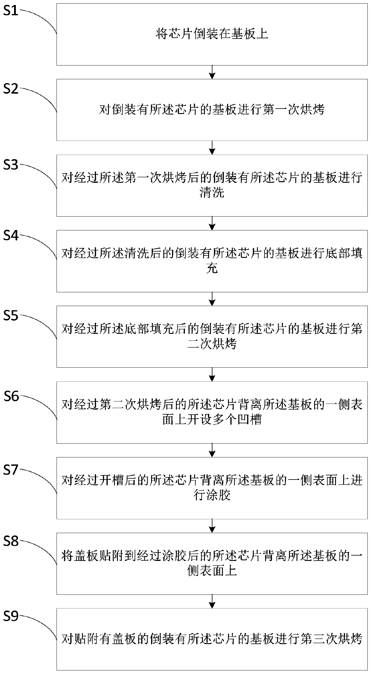
[0047] In order to solve the technical problems proposed in the background technology, figure 1 Show a flow chart of a chip packaging process proposed by the first embodiment of the present invention, such as figure 1 As shown, the process includes the following steps:
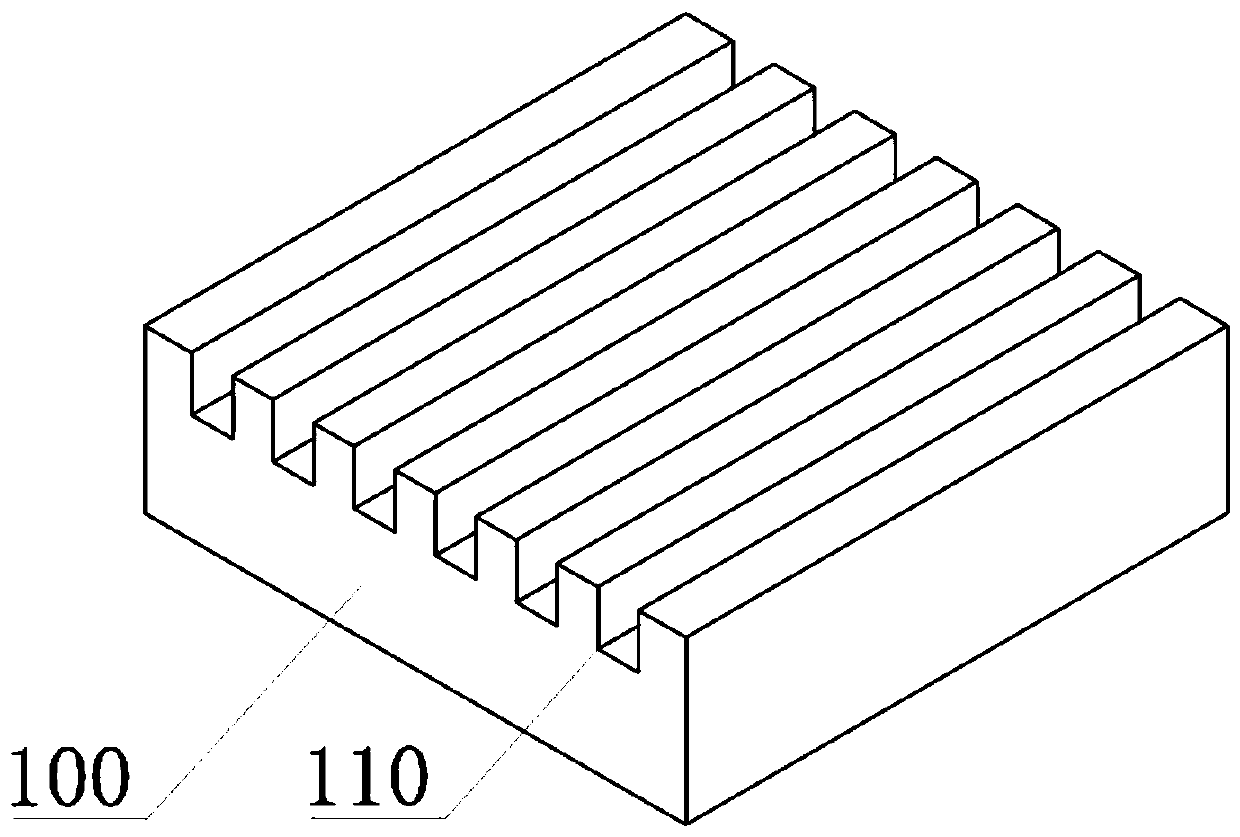
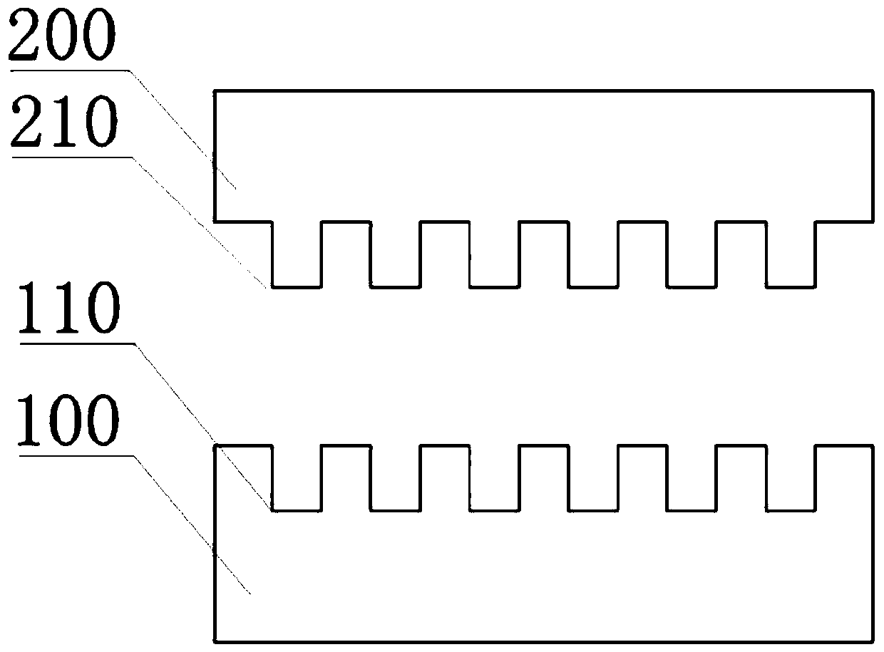
[0048] S1. Flip-chip the chip 100 on the substrate;
[0049] S2. Baking the substrate on which the chip 100 is flip-mounted for the first time;
[0050] S3, cleaning the substrate on which the chip 100 is flip-mounted after the first baking;
[0051] S...
PUM
 Abstract
Description
Claims
Application Information
 - R&D Engineer
- R&D Manager
- IP Professional
- Industry Leading Data Capabilities
- Powerful AI technology
- Patent DNA Extraction
Browse by: Latest US Patents, China's latest patents, Technical Efficacy Thesaurus, Application Domain, Technology Topic.
© 2024 PatSnap. All rights reserved.Legal|Privacy policy|Modern Slavery Act Transparency Statement|Sitemap