Eureka AIR delivers breakthrough ideas for toughest innovation challenges, trusted by R&D personnel around the world.

3D NAND memory cell module, memory and manufacturing method

A 3DNAND, memory cell technology, applied in electrical components, electro-solid devices, semiconductor devices, etc., can solve problems such as the inability to further improve the electron mobility of 3DNAND flash memory

Active Publication Date: 2019-09-24
英特尔半导体(大连)有限公司 +1
View PDF3 Cites 3 Cited by
  • Summary
  • Abstract
  • Description
  • Claims
  • Application Information

AI Technical Summary

Problems solved by technology

However, this method is still limited by the characteristics of the material itself, and cannot further improve the electron mobility in 3D NAND flash memory with more layers.

Method used


Image

  • 3D NAND memory cell module, memory and manufacturing method
  • 3D NAND memory cell module, memory and manufacturing method
  • 3D NAND memory cell module, memory and manufacturing method

Examples


Embodiment Construction

[0018] In the following description, several specific details are set forth. However, embodiments as described herein may be practiced without some of the specific details. In particular embodiments, well-known structures and techniques have not been shown in detail in order not to obscure the understanding of the description.

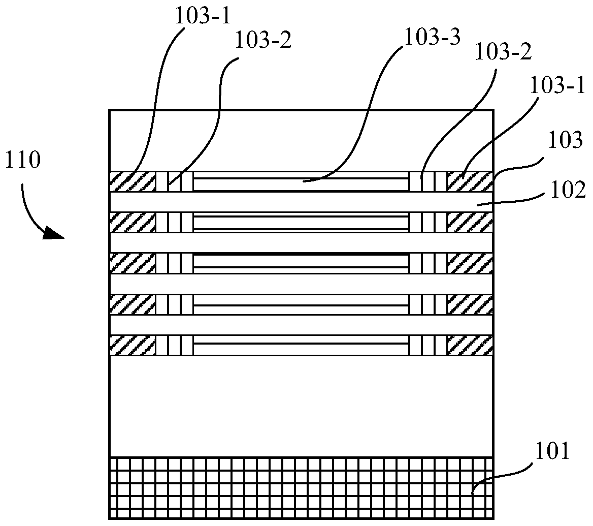
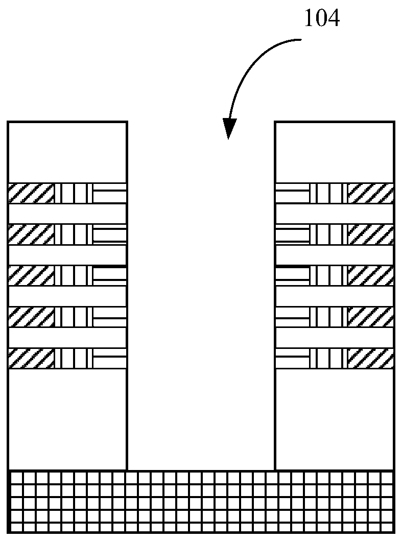
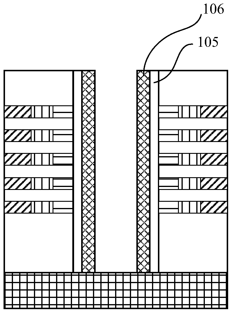
[0019] Figure 1A-Figure 1D A cross-sectional view of an exemplary 3D NAND memory cell deck is shown.

[0020] see Figure 1A , forming a stack structure 110 on the substrate 101 , the stack structure 110 includes insulating material layers 102 and conductive material layers 103 arranged alternately. The conductive material layer 103 is used as a word line. Although only five word lines are shown in the figure, in actual use, the number of word lines may be more or less. In an embodiment, the stack structure 110 may be an OPOP (Oxide / Polysilicon / Oxide / Polysilicon) structure, or an ONON (Oxide / Nitride / Oxide / Nitride) structure, or other structures wi...


PUM


Abstract

The invention provides a 3D NAND memory cell module. The memory cell module comprises a stack structure which comprises an insulating material layer and a conductive material layer which are staggered; a channel layer which extends through the insulating material layer and the conductive material layer along a direction perpendicular to the stack structure; and a semiconductor plug which is arranged at the end part of the channel layer and comprises a conductive reinforcing structure in contact with the channel layer used for improving the electron mobility of the channel layer.

Description

technical field [0001] The invention relates to semiconductor technology, in particular to a 3D NAND storage unit module, a memory and a manufacturing method. Background technique [0002] Memories are commonly used extensively in integrated circuits to store data. Memory generally includes volatile memory and non-volatile memory, where non-volatile memory refers to memory in which data is retained even when power is not applied to the device. A commonly used flash memory (Flash memory) is a non-volatile memory. [0003] A conventional 2D (two-dimensional) NAND (Not AND) flash memory uses a NAND technology implemented based on a two-dimensional plane, which arranges memory cells horizontally in a physical space. With the increasing demand for storage capacity, the storage capacity of 2D NAND flash memory is limited by the physical boundary of the chip, so 3D (three-dimensional) NAND technology came into being. 3D NAND technology stacks storage units in a three-dimensional...

Claims


Application Information

Patent Timeline
Patent Type & Authority Applications(China)
IPC IPC(8): H01L27/11529H01L27/11551H01L27/1157H01L27/11578H10B41/41H10B41/20H10B43/20H10B43/35
CPCH10B41/41H10B41/20H10B43/20H10B43/35
Inventor 焦圣杰
Owner 英特尔半导体(大连)有限公司
Why Eureka
Eureka Blog
Learn More