Gain correction control device
A control device and gain correction technology, applied in gain control, amplification control, analog/digital conversion calibration/testing, etc., can solve the problems of signal blocking, changing impedance matching, difficult gain adjustment, etc., to ensure accuracy, The effect of accurate power measurement
- Summary
- Abstract
- Description
- Claims
- Application Information
AI Technical Summary
Problems solved by technology
Method used
Image

Examples
Embodiment 1
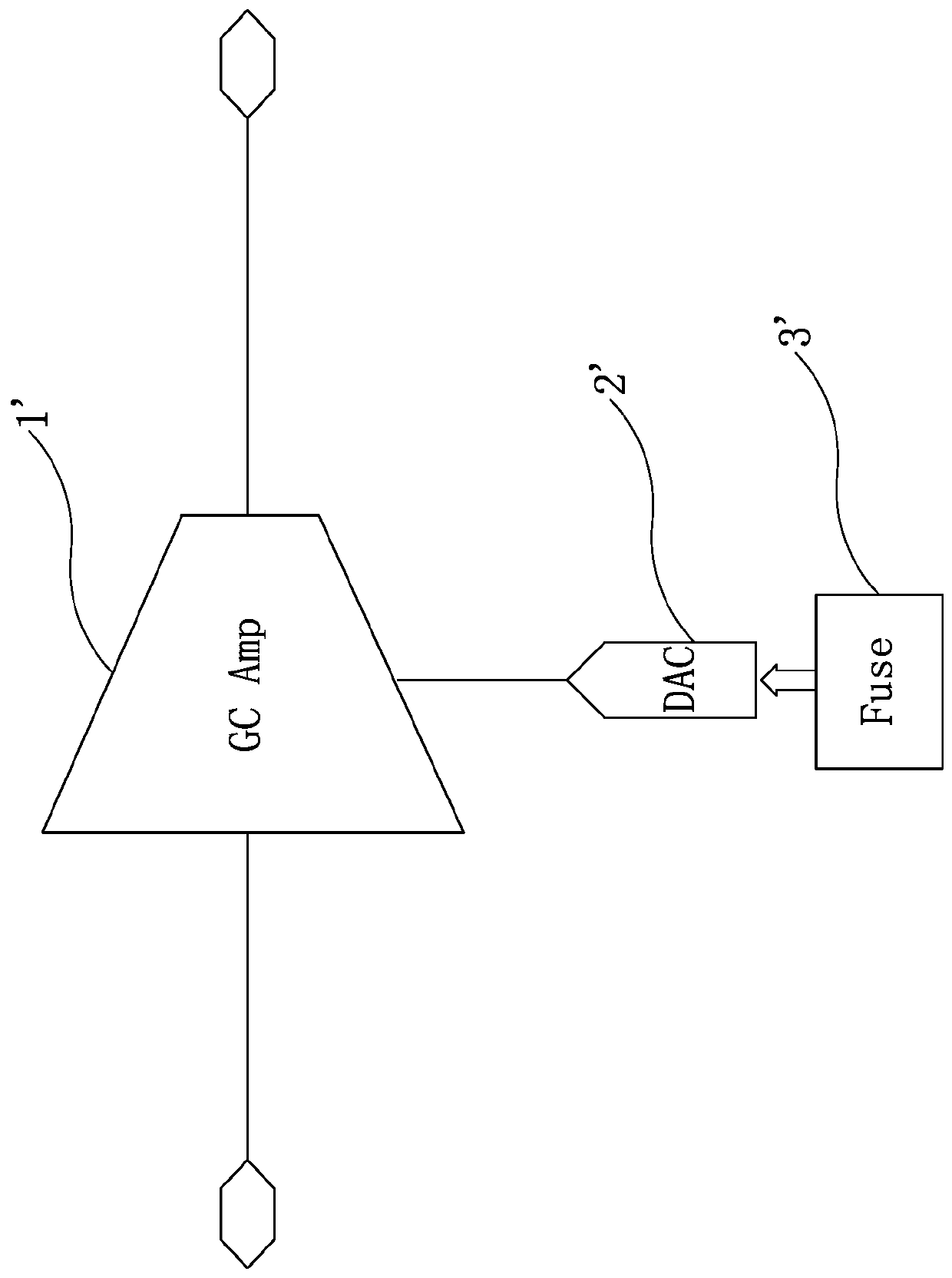
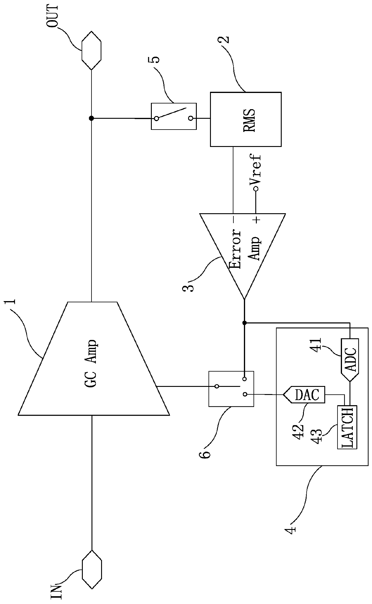
[0024] Such as figure 2 As shown, in Embodiment 1 of the present invention, a gain correction control device includes a signal input terminal IN, a signal output terminal OUT, a gain-adjustable high-frequency signal processing circuit 1, a signal power detection circuit 2, and an error amplifier circuit 3. The correction signal latch circuit 4, the first radio frequency switch 5 and the second radio frequency switch 6; wherein the input terminal of the high frequency signal processing circuit 1 is connected to the signal input terminal IN, and the output terminal of the high frequency signal processing circuit 1 is connected to the first The input terminal of the radio frequency switch 5 and the signal output terminal OUT, the output terminal of the first radio frequency switch 5 is connected to the input terminal of the signal power detection circuit 2, and the output terminal of the signal power detection circuit 2 is connected to the inverting input terminal of the error am...
Embodiment 2
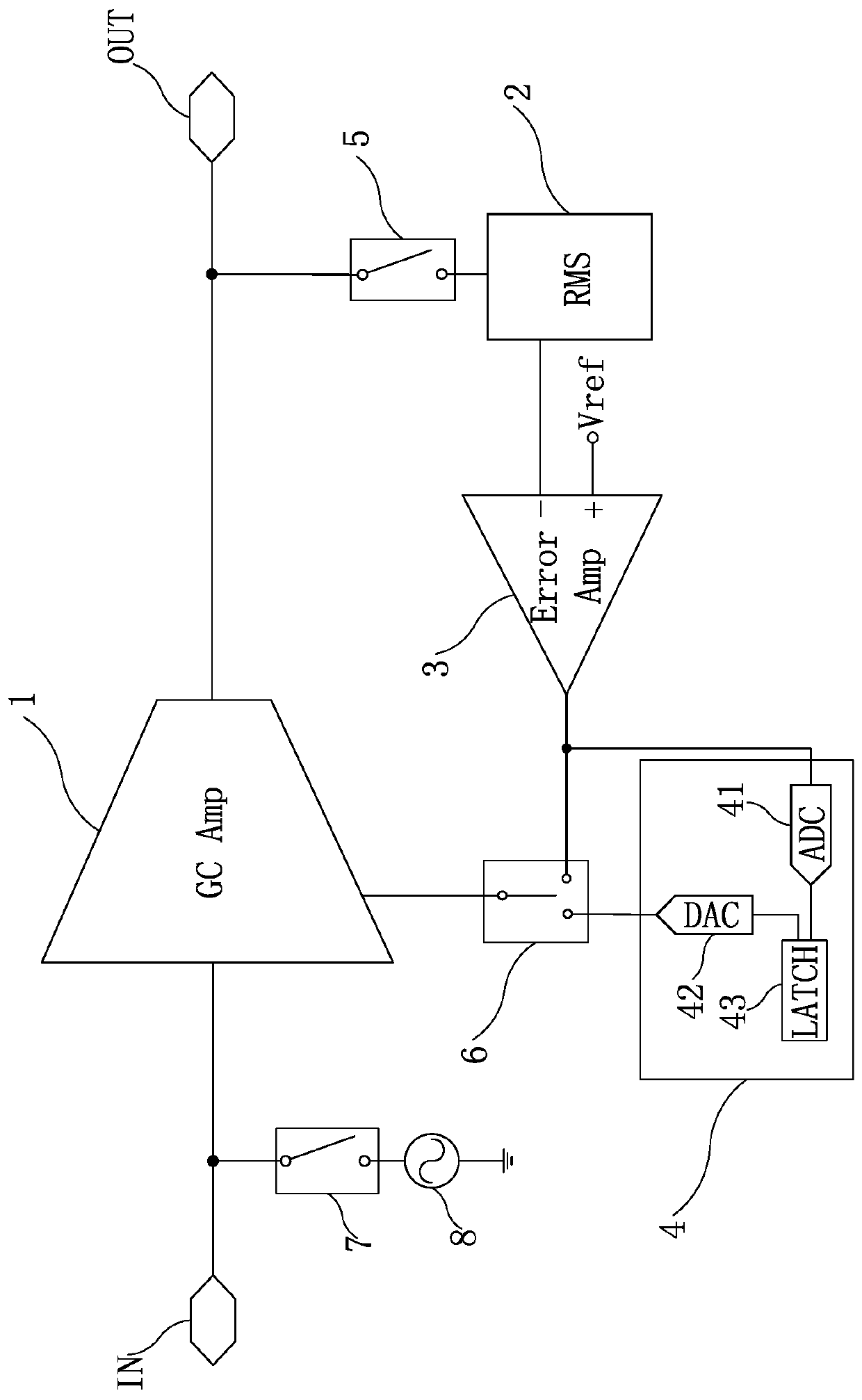
[0030] Such as image 3 As shown, in Embodiment 2 of the present invention, a gain correction control device includes a signal input terminal IN, a signal output terminal OUT, a high-frequency signal processing circuit 1 with adjustable gain, a signal power detection circuit 2, and an error amplifier circuit 3. Correction signal latch circuit 4, first radio frequency switch 5, second radio frequency switch 6, third radio frequency switch 7 and signal source 8 for outputting a test signal; wherein the input terminal of high frequency signal processing circuit 1 is connected The signal input end and the output end of the third radio frequency switch 7, the input end of the third radio frequency switch 7 is connected to the output end of the signal source 8, the output end of the high frequency signal processing circuit 1 is connected to the input end of the first radio frequency switch 5, the first The output end of the radio frequency switch 5 is connected to the input end of t...
PUM
 Abstract
Description
Claims
Application Information
 - Generate Ideas
- Intellectual Property
- Life Sciences
- Materials
- Tech Scout
- Unparalleled Data Quality
- Higher Quality Content
- 60% Fewer Hallucinations
Browse by: Latest US Patents, China's latest patents, Technical Efficacy Thesaurus, Application Domain, Technology Topic, Popular Technical Reports.
© 2025 PatSnap. All rights reserved.Legal|Privacy policy|Modern Slavery Act Transparency Statement|Sitemap|About US| Contact US: help@patsnap.com