Printed circuit board assembly and terminal

A printed circuit board and circuit board technology, applied in the directions of printed circuit components, printed circuit components, stacked printed circuit boards, etc., can solve the problems of easy failure and high stress value.

Active Publication Date: 2019-10-08
VIVO MOBILE COMM CO LTD
View PDF5 Cites 4 Cited by
  • Summary
  • Abstract
  • Description
  • Claims
  • Application Information

AI Technical Summary

Problems solved by technology

[0004] The purpose of the present invention is to provide a printed circuit board assembly and a terminal to solve the problem in the prior art that the single solder joint on the printed circuit board assembly bears too much stress and is prone to failure

Method used


Image

  • Printed circuit board assembly and terminal
  • Printed circuit board assembly and terminal
  • Printed circuit board assembly and terminal

Examples


Embodiment Construction

[0038] The following will clearly and completely describe the technical solutions in the embodiments of the present invention with reference to the accompanying drawings in the embodiments of the present invention. Obviously, the described embodiments are some of the embodiments of the present invention, but not all of them. Based on the embodiments of the present invention, all other embodiments obtained by persons of ordinary skill in the art without creative efforts fall within the protection scope of the present invention.

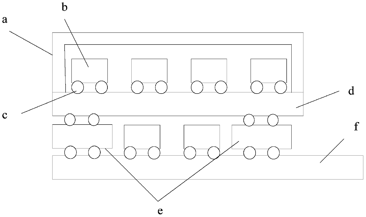
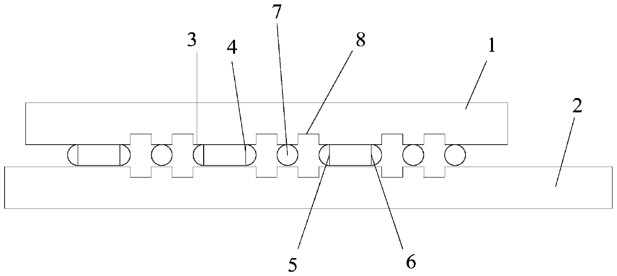
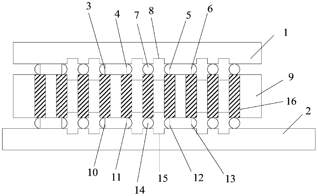
[0039] The present invention aims at the problem that the single solder joint on the printed circuit board assembly bears a relatively large stress value and is prone to failure in the prior art, and provides a printed circuit board assembly, such as Figure 2 to Figure 8 shown, including:

[0040] a first printed circuit board 1;

[0041] A second printed circuit board 2, the second printed circuit board 2 is electrically connected to the first print...


PUM


Abstract

The invention provides a printed circuit board assembly and a terminal. The printed circuit board assembly includes a first printed circuit board, and a second printed circuit board electrically connected with the first printed circuit board by at least four solder joints, wherein the at least four solder joints includes a first solder joint, a second solder joint, a third solder joint and a fourth solder joint, the first solder joint is in communication with the second solder joint, the third solder joint is in communication with the fourth solder joint, at least one solder joint and/or at least one printed circuit board cavity are disposed between the second solder joint and the third solder joint, and the printed circuit board cavity is a recess structure recessed from a surface of a printed circuit board toward the inside. The printed circuit board assembly is advantaged in that the stress on individual solder joints can be scattered, moreover, electromagnetic shielding is providedfor signals of inner solder joints, on the basis of maintaining the scattered solder joint stress and the electromagnetic shielding ability, the gap among the solder joints is enhanced, the space forscaling powder evaporation is improved, and thereby the level of resistance to electromigration is further improved.

Description

technical field [0001] The invention relates to the technical field of terminals, in particular to a printed circuit board assembly and a terminal. Background technique [0002] With the advent and application of 5G, more and more electronic devices need to be carried on the PCB (printed circuit board) of mobile terminals such as smartphones. At the same time, due to the increase in power consumption, the requirements for battery capacity and size are increasing. As a result, in the space in the XY axis direction, the PCB area is becoming more and more insufficient. At present, some products try to stack two or more PCBs in the Z-axis direction, such as figure 1 As shown (a represents the shielding cover, b represents electronic components, c represents the solder ball, d represents the first PCB board, e represents the intermediate connecting frame board, and f represents the second PCB board), use the space in the Z-axis direction to expand the available PCB area. The ...

Claims


Application Information

Patent Timeline
Patent Type & Authority Applications(China)
IPC IPC(8): H05K1/14H05K9/00
CPCH05K1/14H05K1/145H05K9/0022H05K1/144H05K2201/041H05K2201/09036H05K2201/042H05K2201/10378H05K3/3436H05K3/368H05K2201/049H05K2201/09063H05K2201/0949H05K2201/10734H05K2203/0465H05K2201/09609H05K2201/094H05K2201/09627H05K2201/0979H05K1/185H05K1/0216
Inventor 唐后勋
Owner VIVO MOBILE COMM CO LTD
Why Eureka
Try Eureka