Optical waveguide and preparation method thereof

A manufacturing method and optical waveguide technology, applied in the field of integrated optics, can solve problems such as the inability to obtain thicker silicon nitride optical waveguides, the inability to obtain thicker silicon nitride optical waveguides, etc.

Active Publication Date: 2019-10-11
INST OF MICROELECTRONICS CHINESE ACAD OF SCI
View PDF8 Cites 2 Cited by
  • Summary
  • Abstract
  • Description
  • Claims
  • Application Information

AI Technical Summary

Problems solved by technology

[0005] In order to overcome the technical problem of directly digging grooves on silicon dioxide in the prior art, there is a requirement for the width of the grooves, and when the width of the grooves is wider, a thicker silicon nitride optical waveguide cannot be obtained, and then a kind of optical waveguide is provided. Fabrication method that can fabricate wider optical waveguides with a thickness greater than 300 nanometers
[0006] In ord

Method used


Image

  • Optical waveguide and preparation method thereof
  • Optical waveguide and preparation method thereof
  • Optical waveguide and preparation method thereof

Examples


Embodiment 1

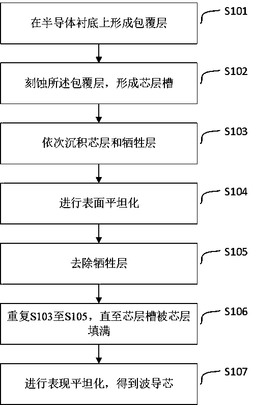
[0066] A flow chart of a manufacturing method for an optical waveguide is shown in figure 1 shown.

[0067] S101, forming a cladding layer on a semiconductor substrate.

[0068] As shown in FIG. 2 ( 1 ), those skilled in the art can form a cladding layer 201 on the semiconductor substrate 200 by using deposition processes such as thermal oxygen, LPCVD, and PECVD.

[0069] Wherein, the semiconductor substrate 200 is an 8-inch silicon substrate, and the cladding layer 201 is a silicon dioxide layer with a thickness between 2 microns and 15 microns, including 2 microns and 15 microns.

[0070] S102. Etching the cladding layer to form grooves in the core layer.

[0071] As shown in FIG. 2 ( 2 ), the cladding layer 201 is etched to form the core layer groove 202 through sequential glue coating, exposure, development, etching, and dry degumming processes, which are common processes in the field.

[0072] In other implementation manners, a hard mask layer may also be grown on the ...


PUM

PropertyMeasurementUnit
Thicknessaaaaaaaaaa
Thicknessaaaaaaaaaa
Thicknessaaaaaaaaaa

Abstract

The invention discloses a preparation method of an optical waveguide, comprising: step (a) of forming a coating layer on a semiconductor substrate; step (b) of etching the coating layer and forming acore layer slot; step (c) of depositing a core layer and a sacrifice layer sequentially; step (d) of performing surface flattening; step (e) of removing the sacrifice layer; step (f) of repeating steps (c) to (e) until the core layer slot is filled with the core layer; and step (g) of performing performance flattening and obtaining a waveguide core. The invention further provides an optical waveguide, comprising a semiconductor substrate; a coating layer located on the semiconductor substrate and being etched with a core layer slot; and a core layer filled in the core layer slot. Adopting thesolution can finally obtain a high-quality silicon nitride strip waveguide with the thickness thereof far exceeding a critical thickness.

Description

technical field [0001] The invention relates to the technical field of integrated optics, in particular to an optical waveguide and a manufacturing method thereof. Background technique [0002] Dielectric waveguides are the basic structural units of integrated optical systems and their components. The dielectric waveguide mainly plays the role of confinement, transmission and coupling of light waves. Dielectric waveguides can be divided into four categories according to the cross-sectional shape: cylindrical waveguides (optical fibers), film (planar) waveguides, rectangular (strip) waveguides and ridge waveguides. Thin-film waveguides and rectangular waveguides are commonly used in integrated optics. There are many types of materials used to form optical waveguides, and silicon nitride is currently a commonly used material for making optical waveguides. [0003] At present, the silicon nitride film growth and preparation methods mainly include PECVD (plasma enhanced chemi...

Claims


Application Information

Patent Timeline
IPC IPC(8): G02B6/132G02B6/136G02B6/122
CPCG02B6/122G02B6/132G02B6/136
Inventor 许庆周章渝李志华
Owner INST OF MICROELECTRONICS CHINESE ACAD OF SCI
Why Eureka
Try Eureka